 | –≠–ª–µ–∫—Ç—Ä–æ–Ω–Ω—ã–π –∫–æ–º–ø–æ–Ω–µ–Ω—Ç: CGB240B | –°–∫–∞—á–∞—Ç—å:  PDF PDF  ZIP ZIP |
CGB 240B
Datasheet
Description:
The CGB240B GaAs power amplifier MMIC has been
especially developed for wireless LAN applications in the
2.4 - 2.5 GHz ISM band, compliant with IEEE 802.11b
standards. The chip is also fully compliant with Bluetooth
class 1 applications and thus can be used in dual-mode
(Bluetooth/WLAN) applications, too.
While providing an effective channel power of 22dBm, the
ACPR is better than -33dB relative to the sinx/x spectral
peak of an IEEE802.11b≠modulated TX signal. Each
CGB240B chip is individually tested for IP3, resulting in
guaranteed ACPR performance.
In a Bluetooth class 1 system, the CGB240B's high power
added efficiency (up to 50%) and single positive supply
operation makes the device ideally suited for handheld
applications. The CGB240B delivers 23 dBm output power
at a supply voltage of 3.2 V, with an overall PAE of 50% in
saturated mode. The output power can be adjusted using
an analog control voltage (V
CTR
). Simple external input-,
interstage-, and output matching circuits are used to adapt
to the different requirements of linearity and harmonic
suppression in various applications2-stage InGaP HBT
power amplifier for WLAN and Bluetooth applications.
Features:
∑ Pout = +23dBm at 3.2 V
∑ ACPR / IP3 tested to be compliant with IEEE802.11b
standard
∑ Fully compliant with Bluetooth requirements (dual-mode
use)
∑ Single voltage supply
∑ Wide operating voltage range 2.0 - 5.5 V
∑ Analog power control with four power steps
1
5
P-TSSOP-10-2
2-Stage Bluetooth & WLAN InGaP HBT Power Amplifier
Applications:
∑ WLAN
∑ IEEE 802.11a
∑ Bluetooth Class 1
Package Outline:
Pin configuration:
1 & 2:
Vc1
3:
RFin
4, 5, & 10:
NC
6:
Vcntrl1
7:
Vcntro2
8 & 9:
Vc2
11 (paddle)
GND
∑ Easy external matching concept
For More Information, Please Visit www.triquint.com
pg.
1/20
Rev 1.3, July 14th, 2003
CGB240B Datasheet
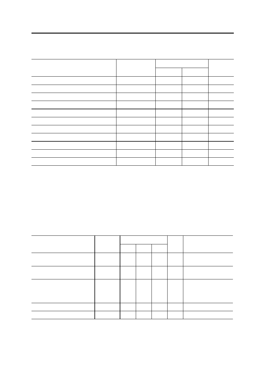
Absolute Maximum Ratings:
Parameter Symbol
Limit
Values
Unit
min.
max.
Max. Supply Voltage CW
V
CC, MAX
0 5.5
V
Max. Supply Voltage Pulsed
V
CCP, MAX
0 5.0
V
Max. Control Voltage
V
CTR, MAX
0 3.5
V
Max. Current Stage 1
I
C1, MAX
0 40
mA
Max. Current Stage 2
I
C2, MAX
0 180
mA
Max. Total Power Dissipation
1
)
P
TOT
650
mW
Max. RF Input Power
2
)
P
IN, MAX
+10
dBm
Max. RF Output Power
2)
P
OUT, MAX
+25
dBm
Operating Temperature Range
T
A
- 40
+85
∞C
Max. Junction Temperature
1)
T
Ch
150
∞C
Storage Temperature
T
Stg
- 55
150
∞C
1
) Thermal resistance between junction and pad 11 ( = heatsink ): R
THCH
= 100 K/W.
2
) No RF input signal should be applied at turn on of DC Power. An output VSWR of 1:1 is assumed.
Typical Electrical Characteristics of CGB240B for IEEE802.11b Applications
(Typical data for CGB240B reference application board, see application note 1 )
T
A
= 25 ∞C; V
CC
= V
CTR
= 3.3 V; f = 2.45 GHz; Z
IN,Board
= Z
OUT,Board
= 50 Ohms
Parameter
Symbol
Limit Values
Unit Test Conditions
min
typ
max
Supply Current
Small-Signal Operation
I
CC, SS
190
mA
P
IN
= - 10 dBm
Power Gain
Small-Signal Operation
G
SS
28
dB
P
IN
= - 10 dBm
Adjacent Channel Power
Ratio
ACPR
≠
33 dBr
P
OUT
= +22dBm
f = f
C
± f
MOD
f
C
= 2.4..2.5 GHz
f
MOD
= 11..22 MHz.
Output Power
P
OUT
+22
dBm
ACPR < -33dBr
Power Added Efficiency
PAE
25
%
P
OUT
= +22dBm
For More Information, Please Visit www.triquint.com
pg.
2/20
Rev 1.3, July 14th, 2003

CGB240B Datasheet
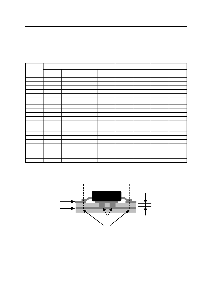
Electrical Characteristics of CGB240B Device used in Bluetooth PA Reference Design
(See Application Note 2)
T
A
= 25 ∞C; V
CC
= 3.2 V; f = 2.4 ... 2.5 GHz; Z
IN,Board
= Z
OUT, Board
= 50 Ohms
Parameter
Symbol
Limit Values
Unit
Test Conditions
min
typ
max
Supply Current
Small-Signal Operation
I
CC,SS
100 130 150
mA P
IN
= - 10 dBm
V
CTR
= 2.5 V
Power Gain
Small-Signal Operation
G
SS
23 25 27
dB P
IN
= - 10 dBm
V
CTR
= 2.5 V
Output Power
Power Step 1
P
OUT,1
7
dBm
P
IN
= + 3 dBm
V
CTR
= 1.15 V
Supply Current
Power Step 1
I
CC,1
15
mA P
IN
= + 3 dBm
V
CTR
= 1.15 V
Power Added Efficiency
Power Step 1
PAE
1
10
% P
IN
= + 3 dBm
V
CTR
= 1.15 V
Output Power
Power Step 2
P
OUT,2
12
dBm
P
IN
= + 3 dBm
V
CTR
= 1.3 V
Supply Current
Power Step 2
I
CC,2
25
mA P
IN
= + 3 dBm
V
CTR
= 1.3 V
Power Added Efficiency
Power Step 2
PAE
2
20
% P
IN
= + 3 dBm
V
CTR
= 1.3 V
Output Power
Power Step 3
P
OUT,3
17
dBm
P
IN
= + 3 dBm
V
CTR
= 1.5 V
Supply Current
Power Step 3
I
CC,3
52
mA P
IN
= + 3 dBm
V
CTR
= 1.5 V
Power Added Efficiency
Power Step 3
PAE
3
32
% P
IN
= + 3 dBm
V
CTR
= 1.5 V
Output Power
Power Step 4
P
OUT,4
22 23 24
dBm P
IN
= + 3 dBm
V
CTR
= 2.5 V
Supply Current
Power Step 4
I
CC,4
130
mA P
IN
= + 3 dBm
V
CTR
= 2.5 V
Power Added Efficiency
Power Step 4
PAE
4
40 50 - % P
IN
= + 3 dBm
V
CTR
= 2.5 V
2
nd
Harm. Suppression
Power Step 4
h
2
-
35
dBc P
IN
= + 3 dBm
V
CTR
= 2.5 V
3
rd
Harm. Suppression
Power Step 4
h
3
-
50
dBc P
IN
= + 3 dBm
V
CTR
= 2.5 V
For More Information, Please Visit www.triquint.com
pg.
3/20
Rev 1.3, July 14th, 2003

CGB240B Datasheet
General Electrical Characteristics of CGB240B
Parameter
Symbol
Limit Values
Unit Test Conditions
min
typ
max
Turn-Off Current
I
CC, OFF
1
uA
V
CC
= 3.2 V
V
CTR
< 0.4 V
No RF Input
Off-State Isolation
S
21, 0
26
dB
P
IN
= + 3 dBm
V
CTR
= 0 V
Rise Time 1
3
)
T
R1
1
µs
V
CC
= 5.0 V
V
CTR
= 0 to 1V Step
Rise Time 2
3)
T
R2
1
µs
V
CC
= 5.0 V
V
CTR
= 0 to 3V Step
Fall Time 1
3)
T
F1
1
µs
V
CC
= 5.0 V
V
CTR
= 1 to 0V Step
Fall Time 2
3)
T
F2
1
µs
V
CC
= 5.0 V
V
CTR
= 3 to 0V Step
Maximum Load VSWR
allowed for 10s
(no damage to device)
VSWR
6
P
IN
= + 5 dBm
V
CC
= 4.8 V
V
CTR
= 2.5 V
Z
IN
= 50 Ohms
3
) Rise time T
R
defined as time between turn-on of V
CTR
voltage until reach of 90% of full output
power level.
Fall time T
F
defined as time between turn-off of V
CTR
voltage until reach of 10% of full output power
level.
Please note: Reduced Vccp, max for pulsed operation applies (see "absolute maximum ratings").
For More Information, Please Visit www.triquint.com
pg.
4/20
Rev 1.3, July 14th, 2003
CGB240B Datasheet
Typical S≠Parameters for IEEE802.11b Operation
T
A
= 25 ∞C; V
CC
= 3.3 V; V
CTR
= 3,3 V; Port 1: RF In (Pin 3); Port 2: RF Out (Pins 8/9)
P
IN
< - 10 dBm; Interstage match and DC bias circuit according to application note 1.
Real
(x1)
Imag
(x1)
Real
(x1)
Imag
(x1)
Real
(x1)
Imag
(x1)
Real
(x1)
Imag
(x1)
0,2
0,31
-0,10
10,46
-2,89
0,0002
0,0001
-0,47
-0,02
0,4
0,29
-0,22
2,51
0,20
0,0001
0,0003
-0,60
0,05
0,6
0,17
-0,31
6,10
1,73
-0,0004
0,0015
-0,61
0,11
0,8
0,04
-0,34
8,57
-0,46
-0,0001
0,0017
-0,60
0,16
1
-0,06
-0,35
9,25
-3,27
0,0003
0,0022
-0,59
0,20
1,2
-0,16
-0,35
8,65
-6,18
0,0004
0,0028
-0,57
0,22
1,4
-0,27
-0,34
7,17
-8,66
0,0007
0,0030
-0,56
0,24
1,6
-0,37
-0,32
5,11
-10,46
0,0008
0,0034
-0,55
0,26
1,8
-0,47
-0,27
2,70
-11,63
0,0012
0,0043
-0,54
0,30
2
-0,57
-0,22
-0,36
-12,67
0,0026
0,0046
-0,50
0,32
2,2
-0,67
-0,11
-3,71
-12,10
0,0025
0,0051
-0,47
0,34
2,3
-0,70
-0,04
-5,32
-11,58
0,0026
0,0049
-0,46
0,36
2,4
-0,73
0,04
-6,88
-10,53
0,0026
0,0048
-0,44
0,37
2,5
-0,74
0,12
-8,18
-9,49
0,0034
0,0051
-0,43
0,39
2,6
-0,74
0,21
-9,23
-8,10
0,0033
0,0055
-0,41
0,41
2,8
-0,69
0,36
-10,40
-4,99
0,0044
0,0059
-0,35
0,44
3
-0,63
0,51
-10,94
-2,12
0,0053
0,0066
-0,30
0,48
3,2
-0,53
0,63
-10,59
0,72
0,0061
0,0067
-0,24
0,50
3,4
-0,41
0,72
-9,16
3,05
0,0084
0,0070
-0,17
0,50
3,6
-0,30
0,77
-7,78
4,53
0,0088
0,0050
-0,12
0,51
3,8
-0,21
0,80
-6,26
5,45
0,0105
0,0051
-0,04
0,51
4
-0,12
0,82
-4,62
6,47
0,0119
0,0033
0,06
0,47
S21
Frequency
(GHz)
S11
S21
S12
Note: Table available as S2P file.
CGB240B
RF signal layer
200µm FR4
epoxy substrate
RF ground plane
Gnd via
Reference planes for
impedance measurements
Figure 1 Ground plane configuration and impedance reference planes.
The impedance reference plane is located at the center of the device pin, assuming
that a continuous microstrip ground plane exists and that low-inductance (e.g. 6-via)
connections of the device's center ground pad (11) to the microstrip ground plane are
present.
For More Information, Please Visit www.triquint.com
pg.
5/20
Rev 1.3, July 14th, 2003

CGB240B Datasheet
Operational Impedances for Bluetooth Application
T
A
= 25 ∞C; V
CC
= 2.8 to 3.2 V; V
CTR
= 2.5 to 2.8 V; f = 2.4 ... 2.5 GHz
P
IN
= + 3 dBm (Large signal operation; PA in compression)
Parameter (Target Data)
Symbol
Typ. Value
Unit
Generator Impedance
4
)
Z
GEN
9 - j 1
Ohms
Interstage Termination
5
)
Z
IS
1 + j 12.5
Ohms
Load Impedance
Z
LOAD
15 + j 3
Ohms
4
)
Generator impedance equals approximately conjugate complex input impedance:
Z
IN
Z
GEN
*
5
)
Z
IS
is the impedance to be presented to the interstage output (pin 1 and pin 2) of the device.
The given load impedance is optimized for output power in saturated mode
(Bluetooth) and does not represent the conjugate complex output impedance of the
device since large signal conditions apply.
CGB240B
RF signal layer
200µm FR4
epoxy substrate
RF ground plane
Gnd via
Reference planes for
impedance measurements
Figure 2 Ground plane configuration and impedance reference planes.
The impedance reference plane is located at the center of the device pin, assuming
that a continuous microstrip ground plane exists and that low-inductance (e.g. 6-via)
connections of the device's center ground pad (11) to the microstrip ground plane are
present.
For More Information, Please Visit www.triquint.com
pg.
6/20
Rev 1.3, July 14th, 2003

CGB240B Datasheet
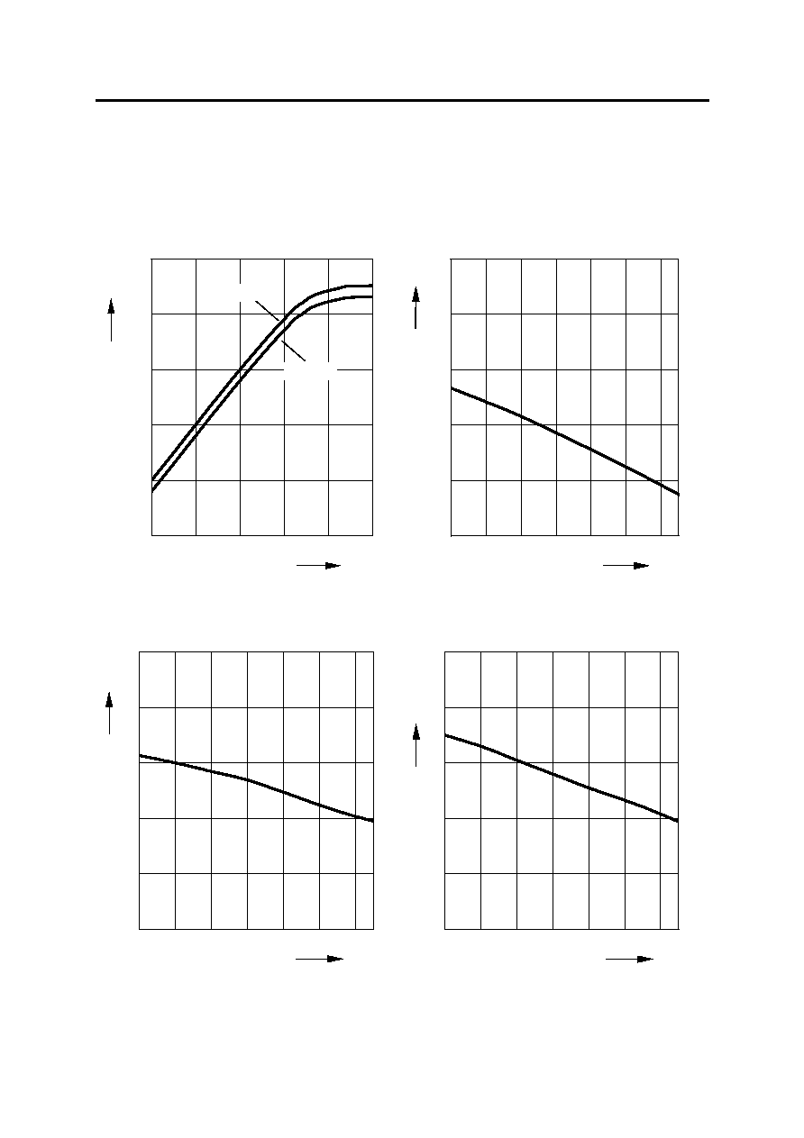
Typical Device Performance for IEEE802.11b Reference Design
(see Application Note 1)
Valid for all plots: T
A
= 25 ∞C; V
CC
= 3.3 V; V
CTR
= 3.3 V; f = 2.45 GHz;
Output Power Compression P
OUT
= f ( P
IN
)
ACPR for IEEE802.11b Modulation
ACPR
IEEE802.11b
= f ( P
OUT
)
20
21
22
23
24
25
-10
-8
-6
-4
-2
0
Input Power
Out
put
Power
dBm
dBm
-40
-35
-30
-25
-20
20
21
22
23
24
Output Power
Ty
pic
a
l
ACP
R
of
Out
put S
i
gnal
dBr
dBm
-33 dBr
Optimum Input Power P
IN
= f ( T
) Output
Power
P
OUT
= f ( T
)
ACPR
IEEE802.11b
< ≠33dBr, P
OUT
>22dBm
ACPR
IEEE802.11b
< ≠33dBr
-7
-6,5
-6
-5,5
-5
-40
-20
0
20
40
60
80
Temperature
Opt
i
mum i
n
put
p
o
w
e
r
for A
C
P
R
<-33d
B
r
dBm
∞C
20,5
21
21,5
22
22,5
-40
-20
0
20
40
60
80
Temperature
P
o
u
t
w
i
th A
C
PR <-
33
dB
r
dBm
∞C
For More Information, Please Visit www.triquint.com
pg.
7/20
Rev 1.3, July 14th, 2003

CGB240B Datasheet
Typical Device Performance for Bluetooth Reference Design
(see Application Note 2)
Valid for all plots: T
A
= 25 ∞C; V
CC
= 3.2 V; V
CTR
= 2.5 V; f = 2.4 ... 2.5 GHz;
Efficiency PAE = f ( V
CC
) Output
Power
P
OUT
= f ( V
CC
)
P
IN
= +3dBm
P
IN
= +3dBm
30,0
35,0
40,0
45,0
50,0
55,0
60,0
2,0
3,0
4,0
5,0
Supply Voltage Vcc
Pow
e
r
A
dded E
f
f
i
c
i
enc
y
P
A
E
%
V
15,0
17,0
19,0
21,0
23,0
25,0
2,0
3,0
4,0
5,0
Supply Voltage Vcc
O
u
t
put
P
o
w
e
r
P
out
dBm
V
Supply Current I
CC
= f ( V
CTR
) Output
Power
P
OUT
= f ( V
CTR
)
P
IN
= +3dBm
P
IN
= +3dBm
0,0
20,0
40,0
60,0
80,0
100,0
120,0
140,0
1,0
1,5
2,0
2,5
3,0
Vctr
S
upply
C
u
r
r
ent
I
c
c
mA
V
Vcc=3.2V
Vcc=2.8V
-10,0
-5,0
0,0
5,0
10,0
15,0
20,0
25,0
1,0
1,5
2,0
2,5
3,
Vctr
O
u
t
put
P
o
w
e
r
P
out
0
dBm
V
Vcc=3.2V
Vcc=2.8V
For More Information, Please Visit www.triquint.com
pg.
8/20
Rev 1.3, July 14th, 2003
CGB240B Datasheet
Typical Device Performance for Bluetooth Reference Design (cont.)
Output Power Compression P
OUT
= f ( P
IN
) Supply
Current
I
CC
= f ( T
A
)
P
IN
= +3dBm, Vcc = 3.2V
0,0
5,0
10,0
15,0
20,0
25,0
-20,0
-15,0
-10,0
-5,0
0,0
5,0
Input Power Pin
O
u
t
p
u
t
Po
w
e
r Po
u
t
dBm
dBm
Vcc=3.2V
Vcc=2.8V
100
110
120
130
140
150
-40
-20
0
20
40
60
80
Ambient Temperature Ta
Tot
a
l
S
u
ppl
y
Current
I
c
c
mA
Deg C
Output Power P
OUT
= f ( T
A
) Small-Signal
Gain
S
21
= f ( T
A
)
P
IN
= +3dBm
P
IN
= -10 dBm, Vcc = 3.2V
20
21
22
23
24
25
-40
-20
0
20
40
60
80
Ambient Temperature Ta
Ou
t
put
P
o
wer P
out
dBm
Deg C
20
22
24
26
28
30
-40
-20
0
20
40
60
80
Ambient Temperature Ta
SS G
a
in
dB
Deg C
For More Information, Please Visit www.triquint.com
pg.
9/20
Rev 1.3, July 14th, 2003

CGB240B Datasheet
Pinning
1
5
P-TSSOP-10-2
Figure 3
CGB240B Outline
Pad Symbol Function
1 V
C1
Supply voltage of 1
st
stage / interstage match
2 V
C1
Supply voltage of 1
st
stage / interstage match
3 RF
IN
RF
input
4 N.C.
5 N.C.
6 V
CTR1
Control voltage 1
st
stage
7 V
CTR2
Control voltage 2
nd
stage
8 V
C2
Supply voltage of 2
nd
stage / RF output
9 V
C2
Supply voltage of 2
nd
stage / RF output
10 N.C.
11 GND
RF and DC ground (pad located on backside of package)
Heatsink. Thermal resistance between junction ≠ pad 11: R
THCH
= 100
K/W.
Functional Diagram
(3)
RFin
(1,2)
Vc1
(8,9) Vc2
(11) Gnd
(6)
Vctr1
(7)
Vctr2
Figure 4
CGB240B Functional Diagram
For More Information, Please Visit www.triquint.com
pg.
10/20
Rev 1.3, July 14th, 2003
CGB240B Datasheet
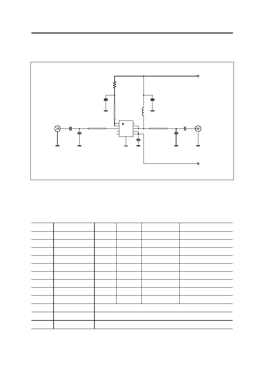
Application Note 1: High Power 22dBm IEEE802.11b Power Amplifier
RF In
RF Out
Vcc
Vctr
C1
C4
C5
TRL1
TRL2
CGB240B
L1
TRL3
R1
C7
C6
C3
C2
1
5
6
10
11
Figure 5
IEEE802.11b WLAN Power Amplifier.
Part Type
Value
Outline
Source
Part
No.
C1
Cer. Capacitor
22 pF
0402
Murata COG
C2
Cer. Capacitor
22 pF
0402
Murata COG
C3
Cer. Capacitor
1.5 pF
0603
AVX ACCU-P
06035J1R5BBT
C4
Cer. Capacitor
2.2 pF
0402
Murata COG
C5
Cer. Capacitor
82 pF
0402
Murata COG
C6
Cer. Capacitor
1 µF
0603
Murata X7R
C7
Cer. Capacitor
1 nF
0402
Murata X7R
L1 Inductor
22
nH
0603 Toko
LL1608≠FS
R1 Resistor
10
0402 Mira
TRL1
6
) Microstrip
Line
l = 2,5 mm; FR4:
r
= 4.8; h = 0,2 mm; w = 0,32 mm
TRL2
8)
Microstrip
Line l = 1,0 mm; FR4:
r
= 4.8; h = 0,2 mm; w = 0,32 mm
TRL3
8)
Microstrip
Line l = 2,8 mm; FR4:
r
= 4.8; h = 0,2 mm; w = 0,32 mm
8
)
Line length measured from corner of capacitor to end of MMIC's lead.
For More Information, Please Visit www.triquint.com
pg.
11/20
Rev 1.3, July 14th, 2003

CGB240B Datasheet
R
1
C6
L
1
C5
C
3
CGB240B
C2
C1
C
4
,,White Dots" =
C7
Ground Vias
RF Out
RF In
(SMA)
(SMA)
Figure 6
Layout of CGB240B evaluation board tuned for IEEE802.11b WLAN
application (see application note 1).
Vc1 and Vc2 are connected together on the PCB.
Vctr1 and Vctr2 are connected together on the PCB.
For More Information, Please Visit www.triquint.com
pg.
12/20
Rev 1.3, July 14th, 2003
CGB240B Datasheet
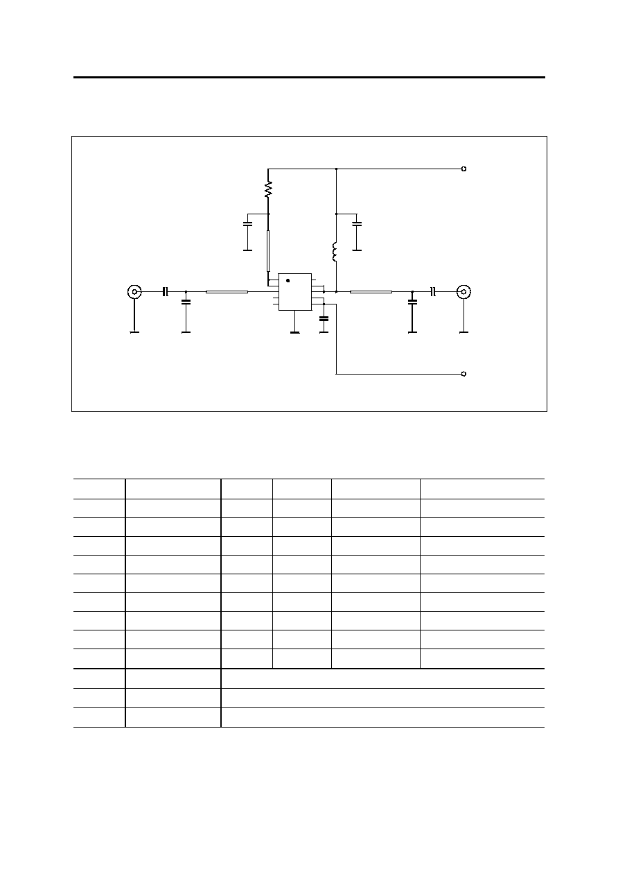
Application Note 2: Bluetooth PA Reference Design using CGB240B
RF In
RF Out
Vcc
Vctr
C1
C4
C5
TRL1
TRL2
CGB240B
L1
TRL3
R1
C7
C6
C3
C2
1
5
6
10
11
Figure 7
Schematic of Bluetooth PA reference design using CGB240B.
Part Type
Value
Outline
Source
Part
No.
C1
Cer. Capacitor
22 pF
0402
Murata COG
C2
Cer. Capacitor
22 pF
0402
Murata COG
C3
7
)
Cer. Capacitor
1.5 pF
0603
AVX ACCU-P
06035J1R5BBT
C4
Cer. Capacitor
2.2 pF
0402
Murata COG
C5
Cer. Capacitor
10 pF
0402
Murata COG
C6
Cer. Capacitor
1 µF
0603
Murata X7R
C7
Cer. Capacitor
1 nF
0402
Murata X7R
L1 Inductor
22
nH
0603 Toko
LL1608≠FS
R1 Resistor
10
0402 Mira
TRL1
8
) Microstrip
Line
l = 2,5 mm; FR4 -
r
= 4.8; h = 0,2 mm; w = 0,32 mm
TRL2
8)
Microstrip
Line l = 1,8 mm; FR4 -
r
= 4.8; h = 0,2 mm; w = 0,32 mm
TRL3
8)
Microstrip
Line l = 4,0 mm; FR4 -
r
= 4.8; h = 0,2 mm; w = 0,32 mm
7
)
Cost optimization might take place by using lower-Q AVX-CU capacitors instead of the AccuP
version. This will lead to better h
2
performance, however resulting in a loss of about 2% PAE.
8
)
Line length measured from corner of capacitor to end of MMIC's lead.
For More Information, Please Visit www.triquint.com
pg.
13/20
Rev 1.3, July 14th, 2003
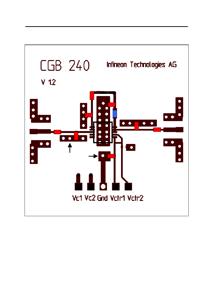
CGB240B Datasheet
R
1
C6
L
1
C5
C
3
CGB240B
C2
C1
C
4
,,White Dots" =
C7
Ground Vias
RF Out
(SMA)
Figure 8
Layout of CGB240B evaluation board using TRL matching
(see application note 2).
Vc1 and Vc2 are connected together on the PCB.
Vctr1 and Vctr2 are connected together on the PCB.
For More Information, Please Visit www.triquint.com
pg.
14/20
Rev 1.3, July 14th, 2003

CGB240B Datasheet
Application Note 3: CGB240B as Bluetooth Power Amplifier using a Lumped
Element Matching Concept
RF In
RF Out
Vcc
C1
C4
L2
CGB240B
L1
L3
C7
C6
C3
C2
1
5
6
10
11
C8
L4
C5
Vctr
Figure 9
CGB240B Bluetooth amplifier using lumped element matching.
Part Type
Value
Outline
Source
Part
No.
C1
Cer. Capacitor
22 pF
0402
Murata COG
C2
Cer. Capacitor
22 pF
0402
Murata COG
C3
Cer. Capacitor
1.5 pF
0603
AVX ACCU-P
06035J1R5BBT
C4
Cer. Capacitor
2.0 pF
0402
Murata COG
C5
Cer. Capacitor
82 pF
0402
Murata COG
C6
Cer. Capacitor
0.1 µF
0603
Murata X7R
C7
Cer. Capacitor
1 nF
0402
Murata X7R
C8
Cer. Capacitor
0.1 µF
0603
Murata X7R
L1 Inductor 22
nH
0603
Toko
LL1005≠FH22NJ
L2 Inductor 1.0
nH
0402
Coilcraft 0402CS-1N0X_BG
L3 Inductor 1.0
nH
0402
Coilcraft 0402CS-1N0X_BG
L4 Inductor 22
nH
0603
Toko
LL1005≠FH22NJ
R1 Jumper
0
0402
For More Information, Please Visit www.triquint.com
pg.
15/20
Rev 1.3, July 14th, 2003

CGB240B Datasheet
R
1
C6
C8
L
1
L
4
C
3
C5
CGB240B
L3
C2
L2
C1
C
4
,,White Dots" =
C7
Ground Vias
RF In
RF Out
(SMA)
(SMA)
Figure 10
Bluetooth PA with lumped element matching
(see application note 3).
A the discrete matching concept shown in figure 10 uses no transmission lines but
only discrete components to provide device matching.
The use of a discrete matching concept saves PCB space an makes the design more
tolerant towards variations of the PCB's
r
, but will lead to a lower output power (typ.
0.3 dB lower) and higher BOM cost.
For More Information, Please Visit www.triquint.com
pg.
16/20
Rev 1.3, July 14th, 2003
CGB240B Datasheet
Description of P-TSSOP-10-2 Package
In order to ensure maximum mounting yield and optimal reliability, special soldering
conditions apply in volume production. Please ask for our information brochure on
details or download the related document (TSSOP10_Soldering_Version01.pdf) from
our website.
The P-TSSOP-10-2 is a level 3 package. International standards for handling this
type of package are described in the JEDEC standard J-STD-033 ,,STANDARD FOR
HANDLING, PACKING, SHIPPING AND USE OF MOISTURE/REFLOW SENSITIVE
SURFACE-MOUNT DEVICES", published May-1999. The original document is
available from the JEDEC website www.jedec.org .
MSL Rating: 1/260C
Pb Free
For More Information, Please Visit www.triquint.com
pg.
17/20
Rev 1.3, July 14th, 2003
CGB240B Datasheet
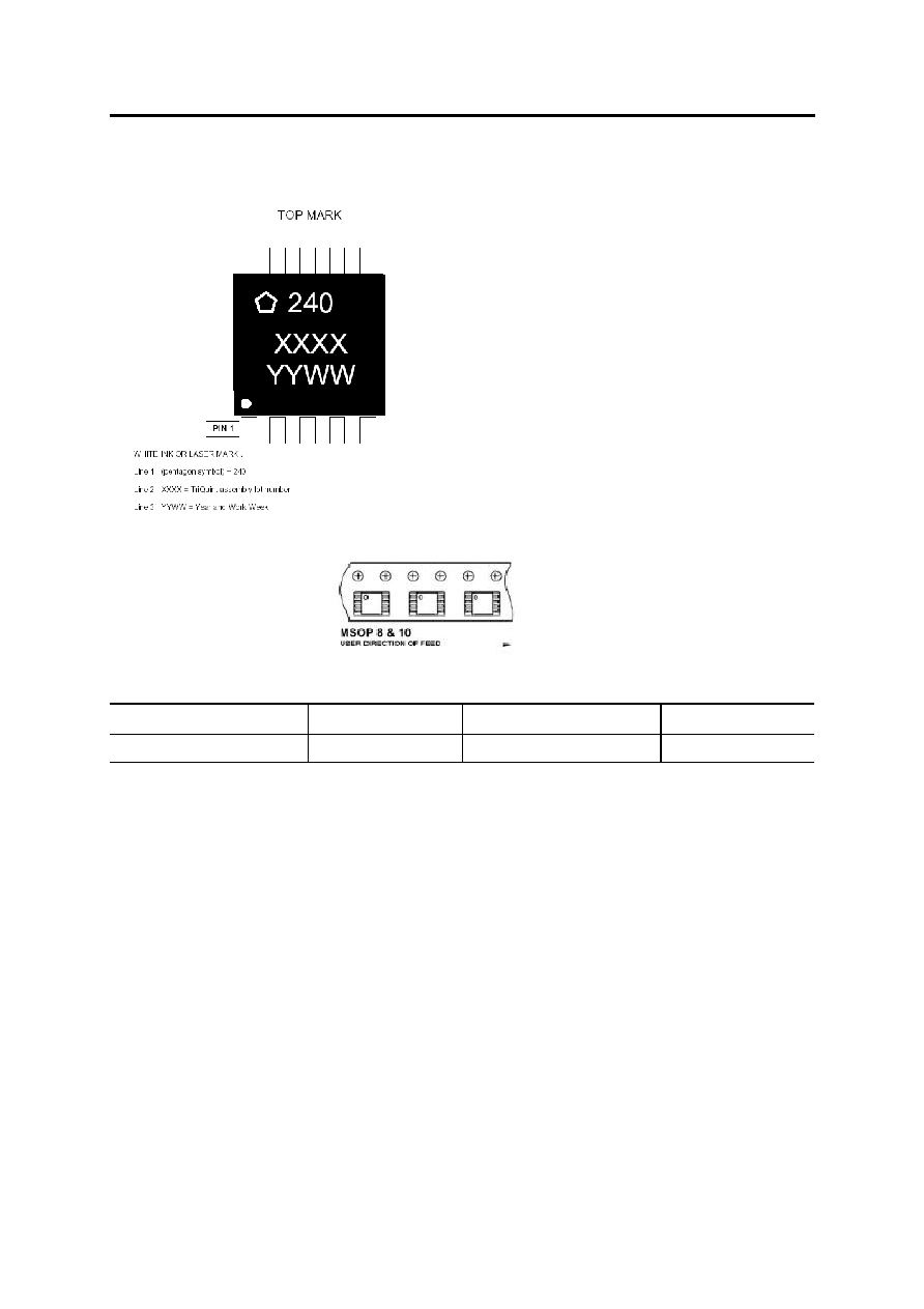
Part Marking:
Part Orientation on Reel:
Ordering Information:
Type Marking
Ordering
Code
Package
CGB240B CGB240B
t.b.d.
P-TSSOP
-
10-2
ESD: Electrostatic discharge sensitive device
Observe handling precautions!
For More Information, Please Visit www.triquint.com
pg.
18/20
Rev 1.3, July 14th, 2003

CGB240B Datasheet
For More Information, Please Visit www.triquint.com
pg.
19/20
Rev 1.3, July 14th, 2003
Published by TriQuint Semiconductor GmbH, Marketing, Konrad-Zuse-Platz 1, D-81829
Munich.
copyright TriQuint Semiconductor GmbH 2003. All Rights Reserved.
As far as patents or other rights of third parties are concerned, liability is only assumed for
components per se, not for applications, processes and circuits implemented within
components or assemblies.
The information describes the type of component and shall not be considered as assured
characteristics.
Terms of delivery and rights to change design reserved.
For questions on technology, delivery, and prices please contact the Offices of TriQuint
Semiconductor in Germany or the TriQuint Semiconductor Companies and Representatives
worldwide.
Due to technical requirements components may contain dangerous substances. For information
on the type in question please contact your nearest TriQuint Semiconductors Office.