 | –≠–ª–µ–∫—Ç—Ä–æ–Ω–Ω—ã–π –∫–æ–º–ø–æ–Ω–µ–Ω—Ç: CSH210R | –°–∫–∞—á–∞—Ç—å:  PDF PDF  ZIP ZIP |

CSH210R
For further information, please visit
www.triquint.com
pg.
1/7
Ver 5; December 16th, 2003
Features:
∑ SPDT Switch for mobile communications:
o Insertion Loss: 0.4 dB @ 2.0 GHz
o Isolation: 20 dB @ 2.0 GHz
o VSWR: 1.3:1
o P0.1dB: +26 dBm
∑ RF-frequency range DC ≠ 2.5 GHz
∑ No supply voltage
∑ Positive control voltage
∑ Small SC-70 plastic package
General Purpose SPDT Switch
Description:
CSH210R is a general purpose single-pole,
double-throw switch device designed for
mobile communications applications such as
cellular and PCS mobile phones, ISM bands,
GPS receivers, L-band satellite terminals,
WLAN and pagers. The device is based on
pHEMT technology and exhibits very low
insertion loss and high intermodulation
performance.
The CSH210R does not need a supply
voltage and switching is accomplished with a
positive control voltage. The device exhibits
excellent VSWRs and isolation and is useable
from DC to 2.5 GHz.
Applications:
∑ General Purpose SPDT
∑
Antenna Diversity Switching
∑ TX-RX Switching
∑ Mobile Phones
∑
ISM and WLAN
∑
L-Band Satellite Terminals
Package Outline:
SC-70
Pin Configuration:
1: RF1
Port
2: GND
3: RF2
Port
4: Control
V2
5: RF
Common
6: Control
V1

CSH210R
Maximum Ratings:
Parameter Symbol
Value
Un
min max
Control Voltage Range
Vcntrl
-5
5
V
RF Input Power
Pin
W
Junction Temperature
@ 30dbm input and 25∞C
Tj 50
∞C
Storage Temperature
Tstg -55 150 ∞C
3
2
it
Exceeding any one or combination of these max ratings may cause permanent damage
AC Electrical Characteristics: (T=25C; Vcntrl=3.0V; Pin=0dBm)**
Parameter Symbol
Test
Condition
min typ max Unit
Insertion Loss RFC-RF1, RFC-
RF2
ILRF 0.5-1.0GHz
1.0-2.0GHz
0.3
0.4
0.45
0.6
dB
Isolation RF1-RF2
ISOL
0.5-1.0GHz
1.0-2.0GHz
19
15
24
20
dB
VSWR* (all ports)
VSWR
DC-2.5GHz
1.3:1
Gate Leakage
IL
0.1
mA
Trise /Tfall (10% RF to 90%RF)
10
nS
Ton /Toff (50% CNTRL -
90%/10%RF)
20
nS
Output Power for 0.1 dB
compression
P0.1dB
DC-2.5GHz 26 dBm
Output Power for 1 dB
compression
P1 DC-2.5GHz 30 dBm
Intermodulation Intercept Point
IP3
Pin=25dBm
Freq.=1.0GHz
56 dBm
*VSWR defined for insertion loss state only
** Performance optimized for 800 MHz to 2GHz operation with 100pF external blocking capacitors
in all RF paths
DC Electrical Characteristics
Parameter min
typ max
Unit
Logic Level Low (State 0)
0
-
0.2
V
Locig Level High (State 1)
2.5
-
5
V
For further information, please visit
www.triquint.com
pg.
2/7
Ver 5; December 16th, 2003

CSH210R
PIN Assignments & Functional Block Diagram
1
2
3
6
4
5
V1
V2
RFC
RF1
RF2
GND
*External DC blocking capacitors required; 100pF on pins 1,3 & 5.
Pin Assignments:
Truth Table:
PIN
Symbol
Abbreviation
Description
1
RF OUTPUT 1
RF1
RF OUTPUT
2
GND
GND
Circuit common and DC return
3
RF OUTPUT 2
RF2
RF OUTPUT
4
V_CONTROL 2
V2
RF OUTPUT 2 control
5
RF COMMON
RFC
Common RF port
6
V_CONTROL 1
V1
RF OUTPUT 1 control
V1 V2 Through
Path
0V
3V
RFC ≠ RF1
3V
0V
RFC ≠ RF2
For further information, please visit
www.triquint.com
pg.
3/7
Ver 5; December 16th, 2003
CSH210R
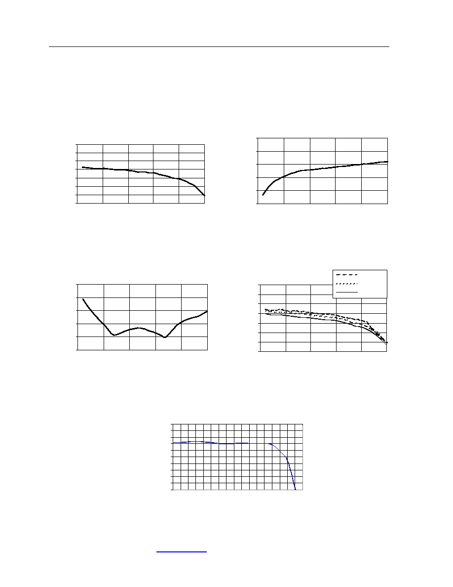
Typical Performance:
(All Ports connected to 50ohms, Pin=0dBm, Vcntrl=3V unless otherwise specified, 100pF blocking capacitors)
Optimized performance can be achieved <0.5GHz by increasing blocking capacitor to >100pF
Optimized performance can be achieved >2.0GHz by decreasing blocking capacitor to <100pF
Insertion Loss Versus Frequency
-0.7
-0.6
-0.5
-0.4
-0.3
-0.2
-0.1
0
0
0.5
1
1.5
2
2.5
Frequency (GHz)
In
ser
t
i
o
n
L
o
ss
(
d
B
)
Isolation versus Frequency
-50
-40
-30
-20
-10
0
0
0.5
1
1.5
2
2.5
Frequency (GHz)
I
s
ol
a
t
i
o
n (
d
B
)
Insertion Loss versus Frequency and
Temperature
-0.7
-0.6
-0.5
-0.4
-0.3
-0.2
-0.1
0
0
0.5
1
1.5
2
2.5
Frequency (GHz)
I
n
s
e
r
t
i
on Los
s
(
d
B)
-30 degC
+25 degC
+85 degC
Input VSWR versus Frequency
-50
-40
-30
-20
-10
0
0
0.5
1
1.5
2
2.5
Frequency (GHz)
WR
VS
Insertion Loss Versus Input Power
-1.0
-0.9
-0.8
-0.7
-0.6
-0.5
-0.4
-0.3
-0.2
-0.1
0.0
15
20
25
30
Input Pow er (dBm )
In
ser
t
i
o
n
L
o
ss
(
d
B
)
For further information, please visit
www.triquint.com
pg.
4/7
Ver 5; December 16th, 2003

CSH210R
Applications Information:
Package Outline ≠ SC-70
Recommended SC-70 Solder Footprint
For further information, please visit
www.triquint.com
pg.
5/7
Ver 5; December 16th, 2003

CSH210R
Evaluation Board Layout
Board Size 0.75" x 1.75"
Board Thickness 0.047", Board Material FR4 Multi-Layer
DC connector
(AMP 5 pin )
RFC
RF1
RF2
SMA RF connector, 3 places
(Johnson Components
142-0711-881)*
*(All Ports connected to 50ohms, Pin=0dBm, Vcntrl=3V unless otherwise specified, 100pF blocking
capacitors)
Optimized performance can be achieved <0.5GHz by increasing blocking capacitor to >100pF
Optimized performance can be achieved >2.0GHz by decreasing blocking capacitor to <100pF
100pF 0402 SMT capacitor, 3 places
(Murata GRP1555C7H100JZ01 or equivalent )
1
2
3
6
4
5
2
1
0
R
1
2
3
6
4
5
2
1
0
R
For further information, please visit
www.triquint.com
pg.
6/7
Ver 5; December 16th, 2003

CSH210R
Additional Information
For latest specifications, additional product information, worldwide sales and distribution locations, and information about TriQuint:
Web: www.triquint.com
Tel: (503) 615-9000
Email:
info_wireless@tqs.com
Fax: (503) 615-8902
For technical questions and additional information on specific applications:
Email:
info_wireless@tqs.com
The information provided herein is believed to be reliable; TriQuint assumes no liability for inaccuracies or omissions. TriQuint assumes no responsibility for the
use of this information, and all such information shall be entirely at the user's own risk. Prices and specifications are subject to change without notice. No patent
rights or licenses to any of the circuits described herein are implied or granted to any third party.
TriQuint does not authorize or warrant any TriQuint product for use in life-support devices and/or systems.
Copyright © 2003 TriQuint Semiconductor, Inc. All rights reserved.
Revision 5-, December 16, 2003
Part Marking:
Part Orientation on Reel:
Ordering Information:
Type
Marking
Package
CSH210R
10R
SC-70
ESD: Electrostatic discharge sensitive device: Observe handling Precautions!
For additional information and latest specifications, see our website: www.triquint.com
pg. 7/7