 | –≠–ª–µ–∫—Ç—Ä–æ–Ω–Ω—ã–π –∫–æ–º–ø–æ–Ω–µ–Ω—Ç: TGA1073A | –°–∫–∞—á–∞—Ç—å:  PDF PDF  ZIP ZIP |

TriQuint Semiconductor Texas : Phone (972)994-8465 Fax (972)994 8504 Web: www.triquint.com
Product Datasheet
1
rev 11/10/98
26- 34 GHz Medium Power Amplifier TGA1073A-SCC
Key Features and Performance
∑
0.25 um pHEMT Technology
∑
19 dB Nominal Gain
∑
25 dBm Nominal Pout @ P1dB
∑
-34.5 dBc IMR3 @ 15.5 dBm SCL
∑
Bias 5 - 7V @ 220 mA
∑
Chip Dimensions 1.95 mm x 1.12 mm
Primary Applications
∑
Point-to-Point Radio
∑
Point-to-Multipoint Communications
∑
LMDS CPE PA
-20
-15
-10
-5
0
5
10
15
20
25
26
27
28
29
30
31
32
33
34
Frequency (GHz)
Ga
i
n
a
nd R
e
turn Los
s
(dB
)
S21
S11
S22
0
5
10
15
20
25
30
26 27 28 29 30 31 32 33 34 35 36
Frequency (GHz)
P1dB (dBm
)
The TriQuint TGA1073A-SCC is a three stage
MPA MMIC design using TriQuint's proven
0.25 um Power pHEMT process. The TGA1073A
is designed to support a variety of millimeter wave
applications including point-to-point digital radio
and LMDS/LMCS.
The three stage design consists of a 200 um input
device driving a 480um interstage device
followed by an 800um output device.
The TGA1073A provides 25dBm nominal
output power at 1dB compression across
26-34GHz. Typical small signal gain is 19 dB.
The TGA1073A requires minimum off-chip
components. Each device is 100% DC and RF
tested on-wafer to ensure performance compliance.
The device is available in chip form.
August 15, 2000

TriQuint Semiconductor Texas : Phone (972)994-8465 Fax (972)994 8504 Web: www.triquint.com
Product Datasheet
2
rev 11/10/98
TGA1073A-SCC
MAXIMUM RATINGS
SYMBOL
PARAMETER 5/
VALUE
NOTES
V
+
POSITIVE SUPPLY VOLTAGE
8 V
I
+
POSITIVE SUPPLY CURRENT
296 mA
1/
P
IN
INPUT CONTINUOUS WAVE POWER
23 dBm
4/
P
D
POWER DISSIPATION
2.37 W
T
CH
OPERATING CHANNEL TEMPERATURE
150
0
C
2/ 3/
T
M
MOUNTING TEMPERATURE
(30 SECONDS)
320
0
C
T
STG
STORAGE TEMPERATURE
-65 to 150
0
C
1/
Total current for all stages.
2/
These ratings apply to each individual FET.
3/
Junction operating temperature will directly affect the device median time to failure (T
M
). For
maximum life, it is recommended that junction temperatures be maintained at the lowest possible
levels.
4/
This value reflects an estimate. Actual value will be inserted as soon as it is determined.
5/
These ratings represent the maximum operable values for the device.
DC SPECIFICATIONS (100%)
(T
A
= 25
∞C + 5 ∞C)
NOTES
SYMBOL
TEST CONDITIONS 2/
LIMITS
UNITS
MIN
MAX
I
MAX3
STD
300
516
mA
I
DSS3
STD
80
376
mA
G
M3
STD
176
424
mS
1/
|V
P1
|
STD
0.5
1.5
V
1/
|V
P2
|
STD
0.5
1.5
V
1/
|V
P3
|
STD
0.5
1.5
V
1/
|V
BVGD1
|
STD
11
30
V
1/
|V
BVGS1
|
STD
11
30
V
1/
V
P
, V
BVGD
, and V
BVGS
are negative.
2/
The measurement conditions are subject to change at the manufacture's discretion (with appropriate notification to the
buyer).
TriQuint Semiconductor Texas : Phone (972)994-8465 Fax (972)994 8504 Web: www.triquint.com
Product Datasheet
3
rev 11/10/98
TGA1073A-SCC
RELIABILITY DATA
PARAMETER
BIAS CONDITIONS
P
DISS
R
JC
T
CH
T
M
V
D
(V)
I
D
(mA)
(W)
(C/W)
(
∞C)
(HRS)
R
JC
Thermal resistance
(channel to backside of c/p)
6
220
1.32
69.4
146.6
1.3 E6
Note: Assumes eutectic attach using 1.5 mil thick 80/20 AuSn mounted to a 20mil CuMo Carrier at 55
∞C
baseplate temperature. Worst case condition with no RF applied, 100% of DC power is
dissipated.
RF SPECIFICATIONS
(T
A
= 25
∞C + 5∞C)
NOTE
TEST
MEASUREMENT
CONDITIONS
VALUE
UNITS
6V @ 220mA
MIN
TYP
MAX
1/
SMALL-SIGNAL
GAIN MAGNITUDE
26 ≠ 33 GHz
17
19
dB
27 GHz
22
24.5
dBm
POWER OUTPUT
AT 1 dB GAIN
COMPRESSION
28 ≠ 33 GHz
23
dBm
26 ≠ 33 GHz
-15
dB
1/
INPUT RETURN LOSS
MAGNITUDE
28 ≠ 32 GHz
-10
dB
26 ≠ 33 GHz
-15
dB
1/
OUTPUT RETURN LOSS
MAGNITUDE
28 ≠ 32 GHz
-10
dB
2/
OUTPUT THIRD ORDER
INTERCEPT
32
dBm
1/
RF probe data is taken at 0.5 GHz steps.
2/ Minimum output third-order-intercept (OTOI) is generally 6dB minimum above the 1dB compression point (P1dB).
Calculations are based on standard two-tone testing with each tone approximately 10dB below the nominal P1dB.
Factors that may affect OTOI performance include device bias, measurement frequency, operating temperature,
output interface and output power level for each tone.

TriQuint Semiconductor Texas : Phone (972)994-8465 Fax (972)994 8504 Web: www.triquint.com
Product Datasheet
4
rev 11/10/98
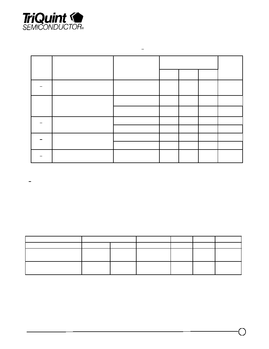
TGA1073A - RF Probe Data Summary - S parameters and P1dB
Vd=6V, Id=220mA, Ta=25C
0
5
10
15
20
25
30
35
26
27
28
29
30
31
32
33
Frequency (GHz)
5th
25th
50th
75th
95th
-40
-35
-30
-25
-20
-15
-10
-5
0
26
27
28
29
30
31
32
33
Frequency (GHz)
5th
25th
50th
75th
95th
0
5
10
15
20
25
30
35
40
28
30
31.5
Frequency (GHz)
5th
25th
50th
75th
95th
-30
-25
-20
-15
-10
-5
0
26
27
28
29
30
31
32
33
Frequency (GHz)
I
npu
t
R
e
t
ur
nL
o
s
s
(
dB)
5th
25th
50th
75th
95th
s11
s21
s22
P1dB
TGA1073A-SCC

TriQuint Semiconductor Texas : Phone (972)994-8465 Fax (972)994 8504 Web: www.triquint.com
Product Datasheet
5
rev 11/10/98
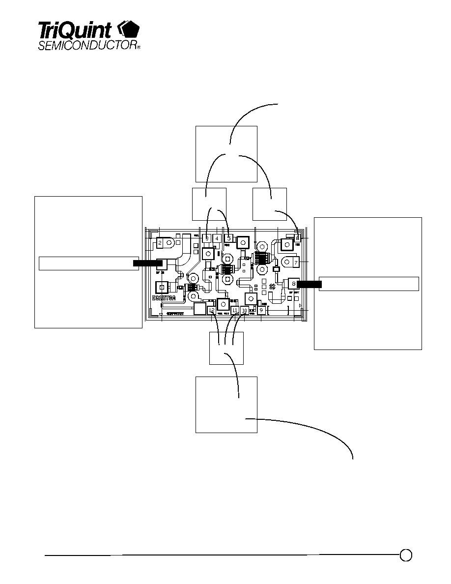
Mechanical Characteristics
TGA1073A-SCC
(VG1)
TriQuint Semiconductor Texas : Phone (972)994-8465 Fax (972)994 8504 Web: www.triquint.com
Product Datasheet
6
rev 11/10/98
.01uF
.01uF
100pF
100pF
100pF
Vg
Vd
Chip Assembly and Bonding Diagram
TGA1073A-SCC
RFin
RFout
TriQuint Semiconductor Texas : Phone (972)994-8465 Fax (972)994 8504 Web: www.triquint.com
Product Datasheet
7
rev 11/10/98
Reflow process assembly notes:
∑= AuSn (80/20) solder with limited exposure to temperatures at or above 300C
∑= alloy station or conveyor furnace with reducing atmosphere
∑= no fluxes should be utilized
∑= coefficient of thermal expansion matching is critical for long-term reliability
∑= storage in dry nitrogen atmosphere
Component placement and adhesive attachment assembly notes:
∑= vacuum pencils and/or vacuum collets preferred method of pick up
∑= avoidance of air bridges during placement
∑= force impact critical during auto placement
∑= organic attachment can be used in low-power applications
∑= curing should be done in a convection oven; proper exhaust is a safety concern
∑= microwave or radiant curing should not be used because of differential heating
∑= coefficient of thermal expansion matching is critical
Interconnect process assembly notes:
∑= thermosonic ball bonding is the preferred interconnect technique
∑= force, time, and ultrasonics are critical parameters
∑= aluminum wire should not be used
∑= discrete FET devices with small pad sizes should be bonded with 0.0007-inch wire
∑= maximum stage temperature: 200C
GaAs MMIC devices are susceptible to damage from Electrostatic Discharge. Proper precautions should
be observed during handling, assembly and test.
TGA1073A-SCC