 | –≠–ª–µ–∫—Ç—Ä–æ–Ω–Ω—ã–π –∫–æ–º–ø–æ–Ω–µ–Ω—Ç: TGA1073G | –°–∫–∞—á–∞—Ç—å:  PDF PDF  ZIP ZIP |

TriQuint Semiconductor Texas : Phone (972)994-8465 Fax (972)994 8504 Web: www.triquint.com
Product Datasheet
1
rev 11/10/98
19 - 27 GHz Medium Power Amplifier TGA1073G-SCC
Key Features and Performance
∑
0.25 um pHEMT Technology
∑
22 dB Nominal Gain
∑
25 dBm Nominal Pout @ P1dB
∑
Bias 5-7V @ 220 mA
∑
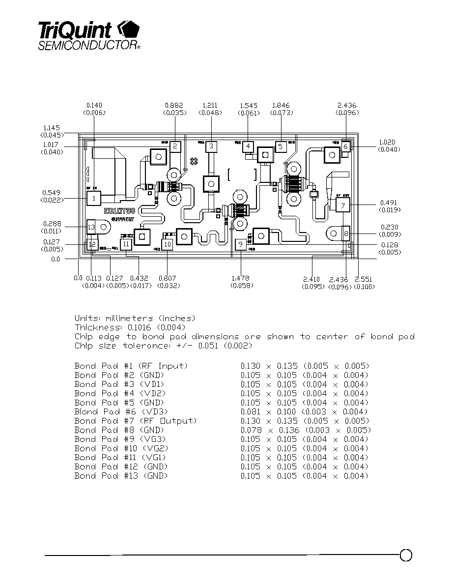
Chip Dimensions 2.55 mm x 1.15mm
Primary Applications
∑
Point-to-Point Radio
∑
Point-to-Multipoint Communications
-30
-25
-20
-15
-10
-5
0
5
10
15
20
25
18
19
20
21
22
23
24
25
26
27
28
Frequency (GHz)
Ga
i
n
a
nd Re
t
u
r
n
Los
s
(
d
B)
S21
S11
S22
0
4
8
12
16
20
24
28
19
20
21
22
23
24
25
26
27
28
29
Frequency (GHz)
P1d
B
(
d
B
m
)
The TriQuint TGA1073G-SCC is a three stage
MPA MMIC design using TriQuint's proven
0.25 um Power pHEMT process. The TGA1073G
is designed to support a variety of millimeter wave
applications including point-to-point digital radio
and point-to-multipoint communications.
The three stage design consists of a 200 um input
device driving a 480um interstage device
followed by an 800um output device.
The TGA1073G provides 25dBm nominal
output power at 1dB compression across
19-27GHz. Typical small signal gain is 22 dB.
The TGA91073G requires minimum off-chip
components. Each device is 100% DC and RF
tested on-wafer to ensure performance compliance.
The device is available in chip form.
August 15, 2000

TriQuint Semiconductor Texas : Phone (972)994-8465 Fax (972)994 8504 Web: www.triquint.com
Product Datasheet
2
rev 11/10/98
August 15, 2000
MAXIMUM RATINGS
SYMBOL
PARAMETER 5/
VALUE
NOTES
V
+
POSITIVE SUPPLY VOLTAGE
8 V
I
+
POSSITIVE SUPPLY CURRENT
296 mA
1/
P
IN
INPUT CONTINUOUS WAVE POWER
23 dBm
4/
P
D
POWER DISSIPATION
2.37 W
T
CH
OPERATING CHANNEL TEMPERATURE
150
0
C
2/ 3/
T
M
MOUNTING TEMPERATURE
(30 SECONDS)
320
0
C
T
STG
STORAGE TEMPERATURE
-65 to 150
0
C
1/
Total current for all stages.
2/
These ratings apply to each individual FET.
3/
Junction operating temperature will directly affect the device median time to failure (T
M
). For maximum
life, it is recommended that junction temperatures be maintained at the lowest possible levels.
4/
This value reflects an estimate. Actual value will be inserted as soon as it is determined.
5/
These ratings represent the maximum operable values for the device
.
DC SPECIFICATIONS (100%)
(T
A
= 25
∞C + 5 ∞C)
NOTES
SYMBOL
TEST CONDITIONS 2/
LIMITS
UNITS
MIN
MAX
I
DSS3
STD
80
376
mA
G
M3
STD
176
424
mS
1/
|V
P1
|
STD
0.5
1.5
V
1/
|V
P2
|
STD
0.5
1.5
V
1/
|V
P3
|
STD
0.5
1.5
V
1/
|V
BVGD1
|
STD
11
30
V
1/
|V
BVGS1
|
STD
11
30
V
1/
V
P
, V
BVGD
, and V
BVGS
are negative.
2/
The measurement conditions are subject to change at the manufacture's discretion (with appropriate
notification to the buyer).

TriQuint Semiconductor Texas : Phone (972)994-8465 Fax (972)994 8504 Web: www.triquint.com
Product Datasheet
3
rev 11/10/98
August 15, 2000
RF SPECIFICATIONS
(T
A
= 25
∞C + 5∞C)
NOTE
TEST
MEASUREMENT
CONDITIONS
VALUE
UNITS
6V @ 220mA
MIN
TYP
MAX
19 GHz
16
20
dB
1/
SMALL-SIGNAL
GAIN MAGNITUDE
20 ≠ 25 GHz
19
23
dB
20 GHz
21
23
dBm
22 GHz
24
25
dBm
POWER OUTPUT
AT 1 dB GAIN
COMPRESSION
23.5 GHz
24
26
dBm
1/
INPUT RETURN LOSS
MAGNITUDE
19 ≠ 25 GHz
-20
dB
1/
OUTPUT RETURN LOSS
MAGNITUDE
19 ≠ 25 GHz
-15
dB
2/
OUTPUT THIRD ORDER
INTERCEPT
32
dBm
1/
RF probe data is taken at 1 GHz steps.
RELIABILITY DATA
PARAMETER
BIAS CONDITIONS
P
DISS
R
JC
T
CH
T
M
V
D
(V)
I
D
(mA)
(W)
(C/W)
(
∞C)
(HRS)
R
JC
Thermal resistance
(channel to backside of
c/p)
6
220
1.32
71.7
149.6
1.0 E6
Note: Assumes eutectic attach using 1.5 mil 80/20 AuSn mounted to a 20mil CuMo Carrier at 55
∞C
baseplate temperature. Worst case condition with no RF applied, 100% of DC power is
dissipated.
TriQuint Semiconductor Texas : Phone (972)994-8465 Fax (972)994 8504 Web: www.triquint.com
Product Datasheet
4
rev 11/10/98
Mechanical Characteristics
August 15, 2000

TriQuint Semiconductor Texas : Phone (972)994-8465 Fax (972)994 8504 Web: www.triquint.com
Product Datasheet
5
rev 11/10/98
.01uF
.01uF
100pF
100pF
100pF
Vg
Vd
Chip Assembly and Bonding Diagram
100pF
August 15, 2000

TriQuint Semiconductor Texas : Phone (972)994-8465 Fax (972)994 8504 Web: www.triquint.com
Product Datasheet
6
rev 11/10/98
Reflow process assembly notes:
∑= AuSn (80/20) solder with limited exposure to temperatures at or above 300C
∑= alloy station or conveyor furnace with reducing atmosphere
∑= no fluxes should be utilized
∑= coefficient of thermal expansion matching is critical for long-term reliability
∑= storage in dry nitrogen atmosphere
Component placement and adhesive attachment assembly notes:
∑= vacuum pencils and/or vacuum collets preferred method of pick up
∑= avoidance of air bridges during placement
∑= force impact critical during auto placement
∑= organic attachment can be used in low-power applications
∑= curing should be done in a convection oven; proper exhaust is a safety concern
∑= microwave or radiant curing should not be used because of differential heating
∑= coefficient of thermal expansion matching is critical
Interconnect process assembly notes:
∑= thermosonic ball bonding is the preferred interconnect technique
∑= force, time, and ultrasonics are critical parameters
∑= aluminum wire should not be used
∑= discrete FET devices with small pad sizes should be bonded with 0.0007-inch wire
∑= maximum stage temperature: 200C
GaAs MMIC devices are susceptible to damage from Electrostatic Discharge. Proper precautions should
be observed during handling, assembly and test.
August 15, 2000