TriQuint Semiconductor Texas : Phone (972)994-8465 Fax (972)994 8504 Web: www.triquint.com
Product Datasheet
September 26, 2002
1
Not Recommended for New Designs
TriQuint Recommends the TGA4509-EPU be used for New Designs
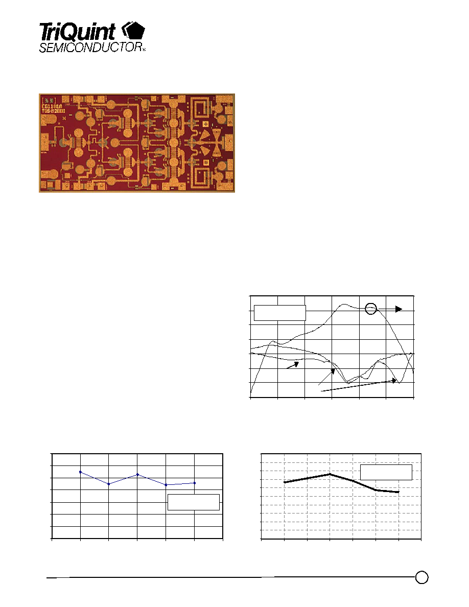
27 - 32 GHz 1W Power Amplifier TGA1172-SCC
Primary Applications
∑
Point-to-Point Radio
∑
Point-to-Multipoint Communications
∑
Ka Band Sat-Com
Key Features
∑
0.25 um pHEMT Technology
∑
16 dB Nominal Gain
∑
29 dBm Nominal P1dB
∑
36dBm OTOI typical at 28GHz
∑
Nominal Input/Output RL < -10 dB
∑
Bias 6 - 7V @ 630 mA
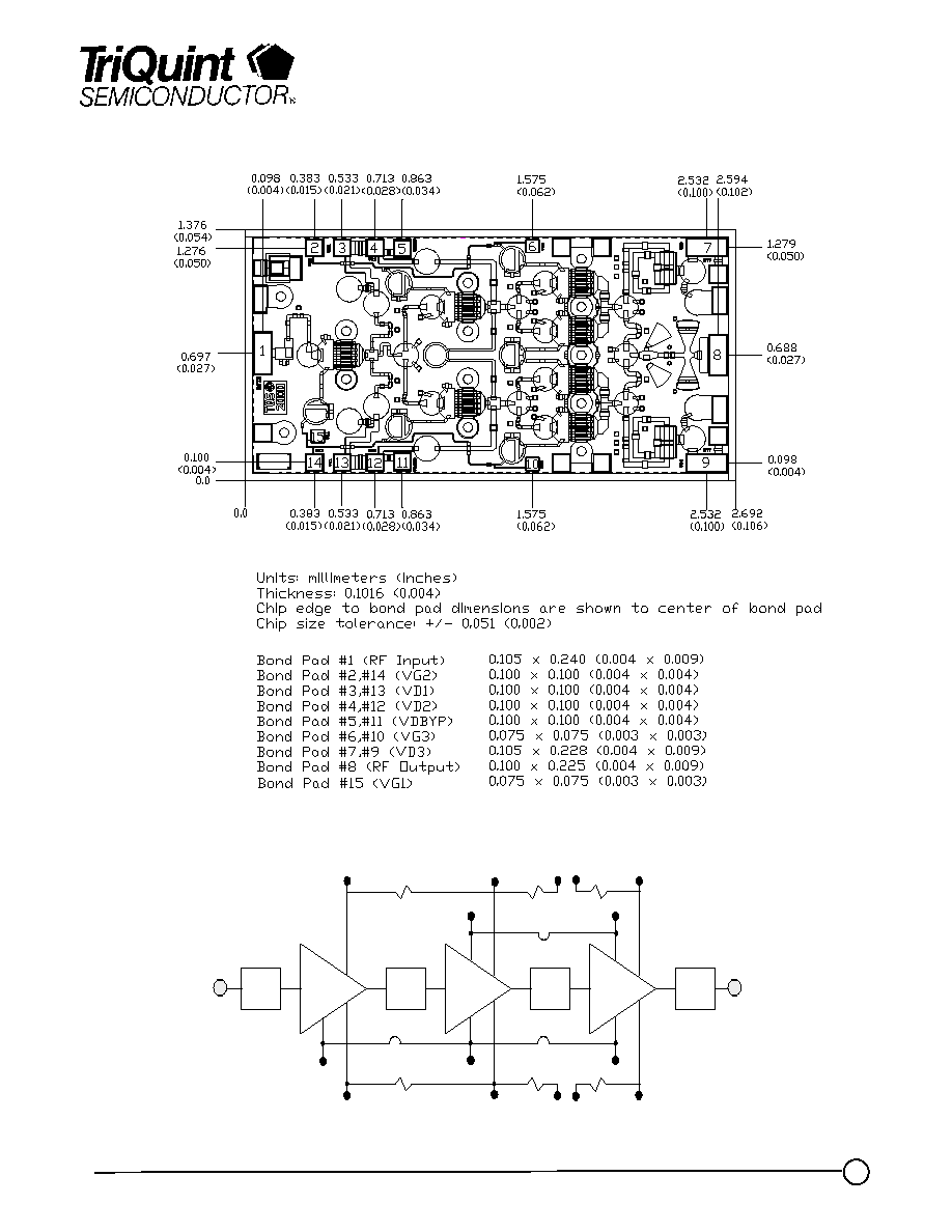
Chip Dimensions 2.7 mm x 1.4 mm x 0.1mm
-20
-15
-10
-5
0
5
10
15
10
15
20
25
30
35
40
-45
-35
-25
-15
-5
5
15
25
S22
S11
S21
R
e
tu
r
n
L
o
s
s
(
d
B
)
Ga
i
n
(d
B
)
Frequency (GHz)
6V, 630 mA
25
26
27
28
29
30
31
32
26
27
28
29
30
31
32
P1
d
B
(
d
Bm
)
Frequency (GHz)
6V, 630 mA
30
31
32
33
34
35
36
37
38
39
40
26
27
28
29
30
31
32
33
()
O
u
tp
u
t
TO
I (d
B
m
)
Frequency (GHz)
6V, 630 mA
Wideband Small Signal Gain
Output Power at P1dB
Output Third Order Intercept
The TriQuint TGA1172-SCC is a three stage
HPA MMIC design using TriQuint's proven
0.25 um Power pHEMT process. The TGA1172
is designed to support a variety of millimeter wave
applications including point-to-point digital radio
and LMDS/LMCS and Ka band satellite ground
terminals.
The three stage design consists of a 600um input
stage driving a 2 x 600um interstage followed by a
4 x 600um output stage.
The TGA1172 provides 29 dBm nominal
output power at 1dB compression across
27-32GHz. Typical small signal gain is 16 dB
with typical Input/Output Return Loss of <-10dB.
The TGA1172 requires minimum off-chip
components. Each device is 100% DC and RF
tested on-wafer to ensure performance
compliance. The device is available in chip form.
Product Description

TriQuint Semiconductor Texas : Phone (972)994-8465 Fax (972)994 8504 Web: www.triquint.com
Product Datasheet
September 26, 2002
2
Not Recommended for New Designs
TriQuint Recommends the TGA4509-EPU be used for New Designs
TGA1172-SCC
TABLE I
MAXIMUM RATINGS
SYMBOL
PARAMETER 4/
VALUE
NOTES
V
+
POSITIVE SUPPLY VOLTAGE
8 V
I
+
POSITIVE SUPPLY CURRENT
840 mA
1/
I
-
NEGATIVE SUPPLY CURRENT
35.2 mA
1/
P
IN
INPUT CONTINUOUS WAVE POWER
23 dBm
P
D
POWER DISSIPATION
5.0 W
T
CH
OPERATING CHANNEL TEMPERATURE
150
0
C
2/ 3/
T
M
MOUNTING TEMPERATURE
(30 SECONDS)
320
0
C
T
STG
STORAGE TEMPERATURE
-65 to 150
0
C
1/
Total current for all stages.
2/
These ratings apply to each individual FET.
3/
Junction operating temperature will directly affect the device median time to failure (T
M
). For maximum life, it is
recommended that junction temperatures be maintained at the lowest possible levels.
4/
These ratings represent the maximum operable values for the device.
TABLE II
DC SPECIFICATIONS (100%)
(T
A
= 25
∞C Nominal)
NOTES
SYMBOL
TEST CONDITIONS 2/
LIMITS
UNITS
MIN
MAX
I
DSS1
STD
60
282
mA
G
M1
STD
132
318
mS
1/
|V
P1
|
STD
0.5
1.5
V
1/
|V
P2-3
|
STD
0.5
1.5
V
1/
|V
P4-7
|
STD
0.5
1.5
V
1/
|V
BVGD1
|
STD
13
30
V
1/
|V
BVGD2-3
|
STD
13
30
V
1/
|V
BVGD4-7
|
STD
13
30
V
1/
|V
BVGS1
|
STD
13
30
V
1/
|V
BVGS2-3
|
STD
13
30
V
1/
|V
BVGS4-7
|
STD
13
30
V
1/
V
P
, V
BVGD
, and V
BVGS
are negative.
2/
The measurement conditions are subject to change at the manufacture's discretion (with appropriate notification to
the buyer).
TriQuint Semiconductor Texas : Phone (972)994-8465 Fax (972)994 8504 Web: www.triquint.com
Product Datasheet
September 26, 2002
3
Not Recommended for New Designs
TriQuint Recommends the TGA4509-EPU be used for New Designs
TGA1172-SCC
TABLE IV
RF SPECIFICATIONS
(T
A
= 25
∞C Nominal)
NOTE
TEST
MEASUREMENT
CONDITIONS
VALUE
UNITS
6V @ 630mA
MIN
TYP
MAX
SMALL-SIGNAL
GAIN MAGNITUDE
27 ≠ 32 GHz
13
16
dB
POWER OUTPUT
AT 1 dB GAIN
COMPRESSION
28 ≠ 32 GHz
27
29
dBm
INPUT RETURN LOSS
MAGNITUDE
27 ≠ 32 GHz
10
dB
OUTPUT RETURN LOSS
MAGNITUDE
27 ≠ 32 GHz
10
dB
OUTPUT THIRD ORDER
INTERCEPT
28 GHz
36
dBm
TABLE V
RELIABILITY DATA
PARAMETER
BIAS CONDITIONS
P
DISS
R
qJC
T
CH
T
M
V
D
(V)
I
D
(mA)
(W)
(C/W)
(
∞C)
(HRS)
R
qJC
Thermal resistance
(channel to backside
of carrier plate)
6
630
3.78
21.35
135.7
3.5E6
Note: Assumes eutectic attach using 1.5 mil 80/20 AuSn mounted to a 20 mil CuMo Carrier at
55
∞C baseplate temperature. Worst case condition with no RF applied, 100% of DC power
is dissipated.
TriQuint Semiconductor Texas : Phone (972)994-8465 Fax (972)994 8504 Web: www.triquint.com
Product Datasheet
September 26, 2002
4
Not Recommended for New Designs
TriQuint Recommends the TGA4509-EPU be used for New Designs
0
2
4
6
8
10
12
14
16
18
20
22
24
26
27
28
29
30
31
32
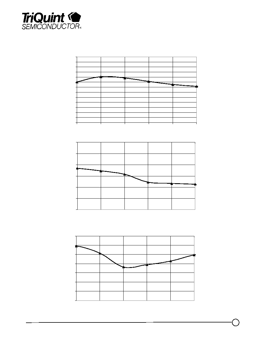
Frequency (GHz)
Gain (
d
B
)
-30
-25
-20
-15
-10
-5
0
27
28
29
30
31
32
Frequency (GHz)
Input Re
turn Los
s
(dB)
-35
-30
-25
-20
-15
-10
-5
0
27
28
29
30
31
32
Frequency (GHz)
Out
put
R
e
t
u
r
n
Los
s
(
d
B
)
TGA1172 Average On-Wafer Small Signal S-Parmeters
Sample Size = 23K devices
TGA1172-SCC
TriQuint Semiconductor Texas : Phone (972)994-8465 Fax (972)994 8504 Web: www.triquint.com
Product Datasheet
September 26, 2002
5
Not Recommended for New Designs
TriQuint Recommends the TGA4509-EPU be used for New Designs
TGA1172-SCC
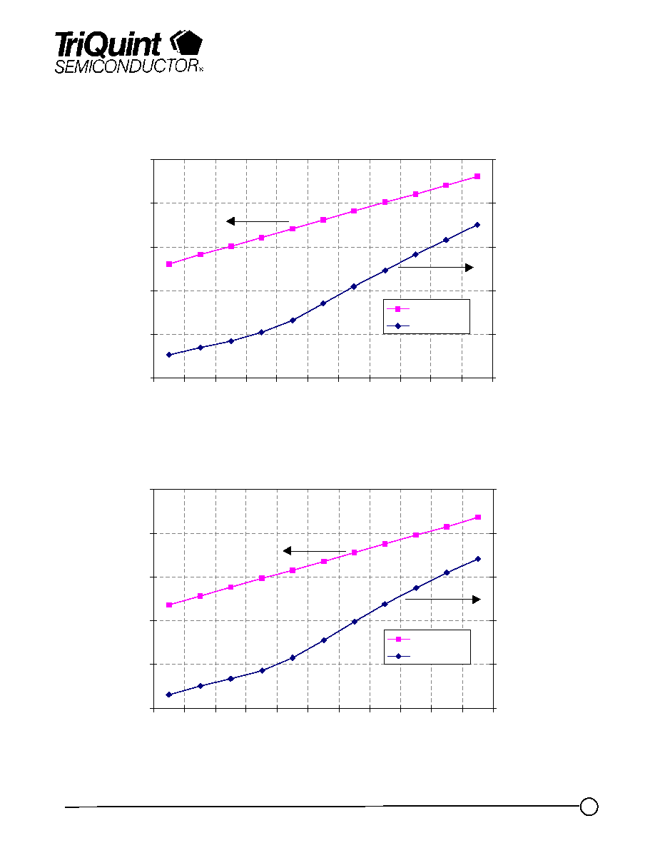
TGA1172 Single tone pout and IMD3 vs Pin
Frequency = 28GHz, 6V, 630 mA
0
5
10
15
20
25
-5
-4
-3
-2
-1
0
1
2
3
4
5
Pin (dBm)
P
out
(
d
Bm
)
-40
-30
-20
-10
0
10
IMD3
(dBm
)
SCL Power
IMD3
TGA1172 Single tone pout and IMD3 vs Pin
Frequency = 31GHz, 6V, 630 mA
0
5
10
15
20
25
-5
-4
-3
-2
-1
0
1
2
3
4
5
Pin (dBm)
P
out
(
d
Bm
)
-40
-30
-20
-10
0
10
IMD3
(dBm
)
SCL Power
IMD3
TriQuint Semiconductor Texas : Phone (972)994-8465 Fax (972)994 8504 Web: www.triquint.com
Product Datasheet
September 26, 2002
6
Not Recommended for New Designs
TriQuint Recommends the TGA4509-EPU be used for New Designs
TGA1172-SCC
Mechanical Drawing
600
mm
1200
mm
2400
mm
Vd1
Vg1
Vd2
Vg2
Vd3
Vg3
Vd1
Vd2
Vg2
Vd3
Vg3
RF
IN
RF
OUT
Amplifier Topology
TriQuint Semiconductor Texas : Phone (972)994-8465 Fax (972)994 8504 Web: www.triquint.com
Product Datasheet
September 26, 2002
7
Not Recommended for New Designs
TriQuint Recommends the TGA4509-EPU be used for New Designs
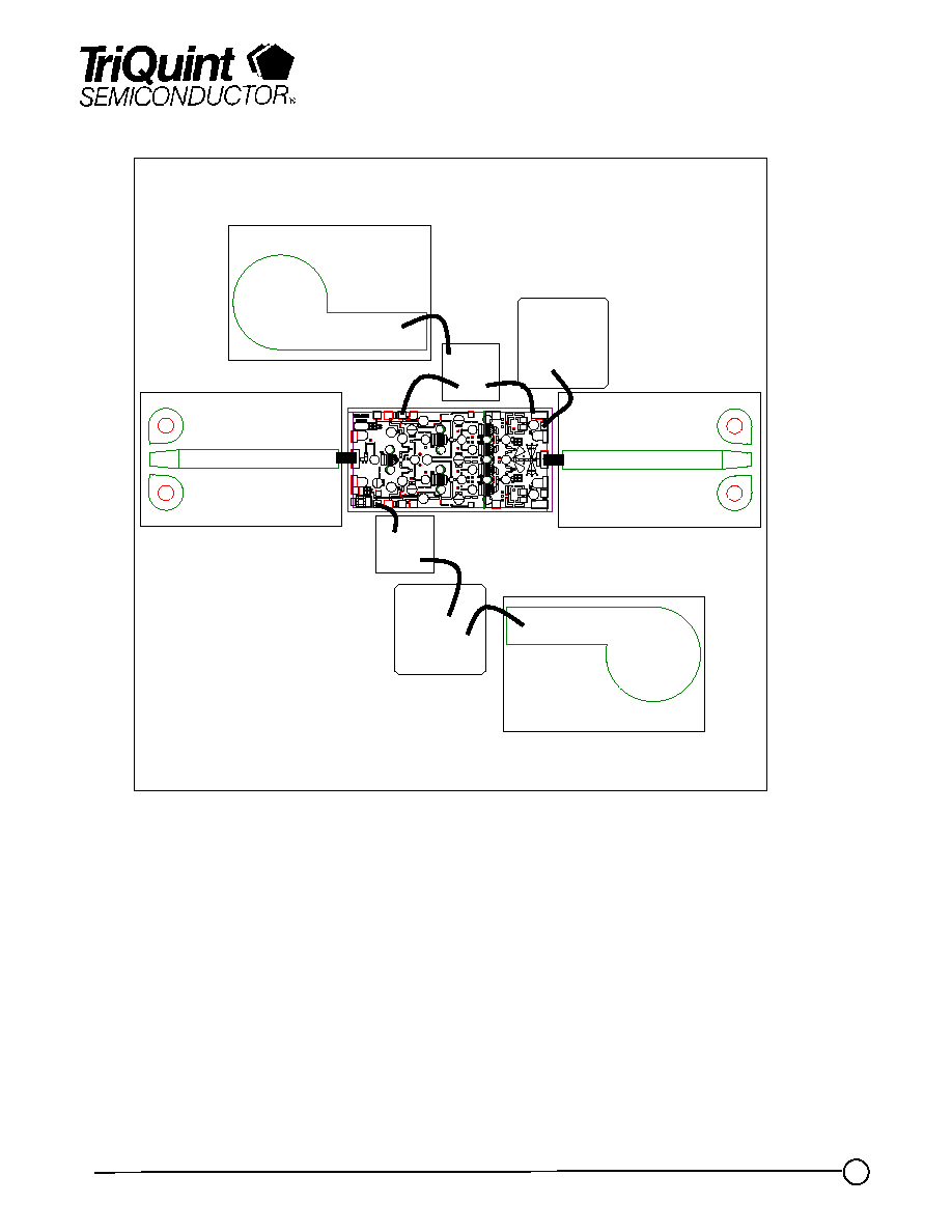
Chip Assembly and Bonding Diagram
GaAs MMIC devices are susceptible to damage from Electrostatic Discharge. Proper precautions should
be observed during handling, assembly and test.
TGA1172-SCC
5mil
Ribbon
100pF
100pF
0.01
mF
0.01
mF
5mil
Ribbon
Vg
Vd
Rf in
Rf out

TriQuint Semiconductor Texas : Phone (972)994-8465 Fax (972)994 8504 Web: www.triquint.com
Product Datasheet
September 26, 2002
8
Not Recommended for New Designs
TriQuint Recommends the TGA4509-EPU be used for New Designs
Assembly Process Notes
GaAs MMIC devices are susceptible to damage from Electrostatic Discharge. Proper precautions should
be observed during handling, assembly and test.
TGA1172-SCC
Reflow process assembly notes:
∑ Use AuSn (80/20) solder with limited exposure to temperatures at or above 300ßC.
∑ An alloy station or conveyor furnace with reducing atmosphere should be used.
∑ No fluxes should be utilized.
∑ Coefficient of thermal expansion matching is critical for long-term reliability.
∑ Devices must be stored in a dry nitrogen atmosphere.
Component placement and adhesive attachment assembly notes:
∑ Vacuum pencils and/or vacuum collets are the preferred method of pick up.
∑ Air bridges must be avoided during placement.
∑ The force impact is critical during auto placement.
∑ Organic attachment can be used in low-power applications.
∑ Curing should be done in a convection oven; proper exhaust is a safety concern.
∑ Microwave or radiant curing should not be used because of differential heating.
∑ Coefficient of thermal expansion matching is critical.
Interconnect process assembly notes:
∑ Thermosonic ball bonding is the preferred interconnect technique.
∑ Force, time, and ultrasonics are critical parameters.
∑ Aluminum wire should not be used.
∑ Discrete FET devices with small pad sizes should be bonded with 0.0007-inch wire.
∑ Maximum stage temperature is 200ßC.