 | –≠–ª–µ–∫—Ç—Ä–æ–Ω–Ω—ã–π –∫–æ–º–ø–æ–Ω–µ–Ω—Ç: TGA2505 | –°–∫–∞—á–∞—Ç—å:  PDF PDF  ZIP ZIP |

TriQuint Semiconductor Texas Phone : (972)994-8465 Fax: (972)994-8504 Web: www.triquint.com
Advance Product Information
April 5, 2006
1
13 - 17 GHz 2.5 Watt, 25dB Power Amplifier TGA2505
Key Features and Performance
∑
34 dBm Midband Pout
∑
25 dB Nominal Gain
∑
7 dB Typical Input Return Loss
∑
12 dB Typical Output Return Loss
∑
Built-in Directional Power Detector
with Reference
∑
0.25µm pHEMT Technology
∑
Bias Conditions: 7V, 640mA
∑
Chip dimensions:
2.03 x 1.39 x 0.10 mm
(0.080 x 0.055 x 0.004 inches)
Preliminary Measured Performance
Bias Conditions: Vd=7V Id=640mA
Primary Applications
∑
VSAT
∑
Point-to-Point
0
5
10
15
20
25
30
11
12
13
14
15
16
17
18
19
Frequency (GHz)
S21 (
d
B)
-20
-15
-10
-5
0
5
10
S11,
S22 (
d
B)
S21
S11
S22
25
26
27
28
29
30
31
32
33
34
35
11
12
13
14
15
16
17
18
19
Frequency (GHz)
Psat
(
d
Bm)
10
15
20
25
30
35
40
45
50
55
60
PAE@Psat (%)
Psat
PAE
Note: This device is early in the characterization process prior to finalizing all electrical specifications. Specifications are subject to
change without notice.

TriQuint Semiconductor Texas Phone : (972)994-8465 Fax: (972)994-8504 Web: www.triquint.com
Advance Product Information
April 5, 2006
2
TGA2505
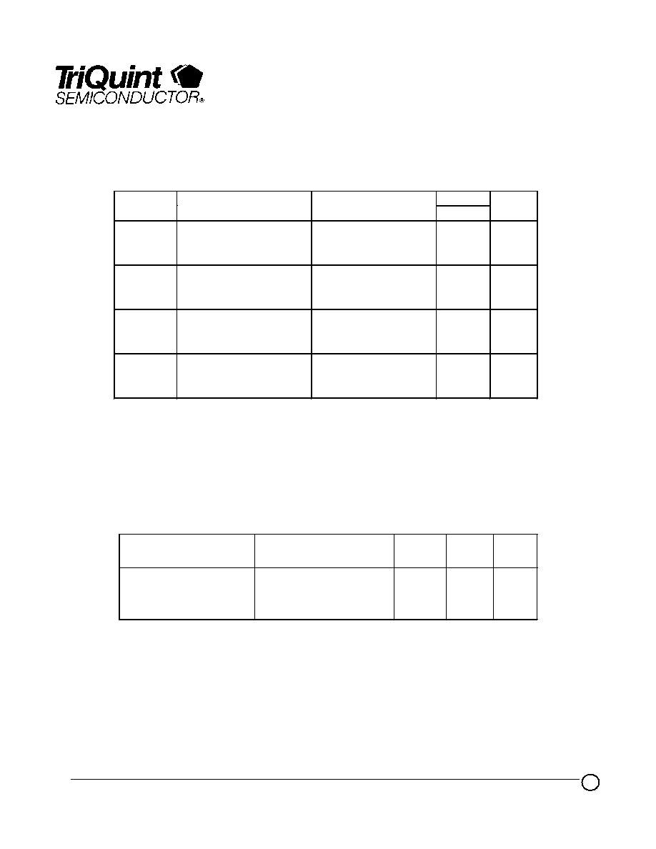
TABLE I
MAXIMUM RATINGS
Symbol
Parameter 1/
Value
Notes
V
+
Positive Supply Voltage
8 V
2/
V
-
Negative Supply Voltage Range
-5V to 0V
I
+
Positive Supply Current (Quiescent)
1300 mA
2/
| I
G
|
Gate Supply Current
18 mA
P
IN
Input Continuous Wave Power
24 dBm
2/
P
D
Power Dissipation
6.43 W
2/ 3/
T
CH
Operating Channel Temperature
150
0
C
4/ 5/
T
M
Mounting Temperature
(30 Seconds)
320
0
C
T
STG
Storage Temperature
-65 to 150
0
C
1/
These ratings represent the maximum operable values for this device.
2/
Combinations of supply voltage, supply current, input power, and output power
shall not exceed P
D
.
3/
When operated at this bias condition with a base plate temperature of 70
∞
C, the
median life is reduced from 8.9E+6 to 1E+6.
4/
These ratings apply to each individual FET.
5/
Junction operating temperature will directly affect the device median time to
failure (T
M
). For maximum life, it is recommended that junction temperatures be
maintained at the lowest possible levels.
TABLE II
DC PROBE TEST
(TA = 25
∞
C, Nominal)
LIMITS
NOTES
SYMBOL
MIN
MAX
UNITS
1/
I
DSS
80
381
mA
1/
G
M
175
425
mS
2/
|V
P
|
0.5
1.5
V
2/
|V
BVGS
|
8
30
V
2/
|V
BVGD
|
13
30
V
1/ Measurements are performed on a 800
µ
m FET.
2/ V
P
, V
BVGD
, and V
BVGS
are negative.
TriQuint Semiconductor Texas Phone : (972)994-8465 Fax: (972)994-8504 Web: www.triquint.com
Advance Product Information
April 5, 2006
3
TABLE III
RF CHARACTERIZATION TABLE
(T
A
= 25
q
C, Nominal)
(Vd = 7V, Id = 640mA
r
5%)
LIMITS
SYMBOL
PARAMETER
TEST CONDITION
TYP
UNITS
Gain
Small Signal Gain
F = 13 ≠ 17 GHz
25
dB
IRL
Input Return Loss
F = 13 ≠ 17 GHz
7
dB
ORL
Output Return Loss
F = 13 ≠ 17 GHz
12
dB
PWR
Output Power @
Pin = +15 dBm
F = 13 ≠ 17 GHz
34
dBm
Note: Table III Lists the RF Characteristics of typical devices as determined by
fixtured measurements.
TABLE IV
THERMAL INFORMATION
PARAMETER
TEST CONDITION
T
CH
(
q
C)
R
T
jc
(
q
C/W)
MTTF
(HRS)
R
jc
Thermal Resistance
(Channel to Backside)
V
D
= 7V
I
D
= 640mA
P
D
= 4.48W
125.74
12.44
8.9E+6
Note: Assumes eutectic attach using 1.5mil 80/20 AuSn mounted to a 20mil CuMo carrier at
70
∞
C baseplate temperature. Worst case condition with no RF applied, 100% of DC
power is dissipated.
TGA2505

TriQuint Semiconductor Texas Phone : (972)994-8465 Fax: (972)994-8504 Web: www.triquint.com
Advance Product Information
April 5, 2006
4
Typical Fixtured Performance
15
16
17
18
19
20
21
22
23
24
25
26
27
28
29
30
11
12
13
14
15
16
17
18
19
Frequency (GHz)
S21 (dB)
-30
-25
-20
-15
-10
-5
0
11
12
13
14
15
16
17
18
19
Frequency (GHz)
S11,
S22 (dB)
S11
S22
TGA2505

TriQuint Semiconductor Texas Phone : (972)994-8465 Fax: (972)994-8504 Web: www.triquint.com
Advance Product Information
April 5, 2006
5
Typical Fixtured Performance
30
30.5
31
31.5
32
32.5
33
33.5
34
34.5
35
11
12
13
14
15
16
17
18
19
Frequency (GHz)
Pout (dBm)
Psat
P2dB
10
15
20
25
30
35
40
11
12
13
14
15
16
17
18
19
Frequency (GHz)
PAE (%
)
PAE @ Psat
PAE @ P2dB
TGA2505

TriQuint Semiconductor Texas Phone : (972)994-8465 Fax: (972)994-8504 Web: www.triquint.com
Advance Product Information
April 5, 2006
6
Typical Fixtured Performance
17
19
21
23
25
27
29
31
33
35
37
-5
-3
-1
1
3
5
7
9
11
13
15
17
19
Input power (dBm)
Out
put
P
o
we
r (
d
Bm)
600
800
1000
1200
1400
1600
1800
2000
2200
2400
2600
Id (
m
A)
13.5 GHz
14.0 GHz
14.5 GHz
TGA2505

TriQuint Semiconductor Texas Phone : (972)994-8465 Fax: (972)994-8504 Web: www.triquint.com
Advance Product Information
April 5, 2006
7
Typical Fixtured Performance
-36
-30
-24
-18
-12
-6
0
6
12
18
16
18
20
22
24
26
28
30
Output power/tone (dBm)
IMD3 (dBm)
13GHz
14GHz
15GHz
35
36
37
38
39
40
41
42
43
44
45
11
12
13
14
15
16
17
18
19
Frequency (GHz)
I
P
3 Avg (dBm
)
TGA2505

TriQuint Semiconductor Texas Phone : (972)994-8465 Fax: (972)994-8504 Web: www.triquint.com
Advance Product Information
April 5, 2006
8
Mechanical Drawing
!
"
#
$
%
&
'
√
(&√#
%($√!&
!("√$
%√#
%('√!&
!'"√$
√
(
$
√
#
#
(
#
√
(
&
&
√
"
(
"
$
√
&
%
!
"
√
'
"
&
#
√
$
'
#
(
√
"
"
'
!
√
&
!
"(√$$
8QLWV PLOOLPHWHUV LQFKHV�
7KLFNQHVV �
&KLS HGJH WR ERQG SDG GLPHQVLRQV DUH VKRZQ WR FHQWHU RI ERQG SDG
&KLS VL]H WROHUDQFH �
*1' ,6 %$&.6,'( 2) 00,&
%RQG SDG
5) ,QSXW�
[ [ �
%RQG SDG
9UHI�
[ [ �
%RQG SDG
9G�
[ [ �
%RQG SDG
9G�
[ [ �
%RQG SDG
5) 2XWSXW�
[ [ �
%RQG SDG
9GHW�
[ [ �
%RQG SDG
9J�
[ [ �
%RQG SDG
9J�
[ [ �
TGA2505

TriQuint Semiconductor Texas Phone : (972)994-8465 Fax: (972)994-8504 Web: www.triquint.com
Advance Product Information
April 5, 2006
9
Power Detector
40K
:
40K
:
+5V
Vdet
Vref
50
:
RF out
DUT
5pF
MMIC
External
TGA2505 Power Detector @ 14GHz
0
0.1
0.2
0.3
0.4
0.5
0.6
0
10
20
30
40
50
60
sqrt Pout (mW^0.5)
Vref-Vdet (V)
(20 dBm)
(26 dBm)
(29.5 dBm) (32 dBm) (34 dBm)
TGA2505

TriQuint Semiconductor Texas Phone : (972)994-8465 Fax: (972)994-8504 Web: www.triquint.com
Advance Product Information
April 5, 2006
10
Chip Assembly & Bonding Diagram
GaAs MMIC devices are susceptible to damage from Electrostatic Discharge. Proper precautions should
be observed during handling, assembly and test.
100pF
Vg
Input TFN
Output TFN
100pF
Vd
Off chip
R=10
:
Off chip
C=0.1
P
F
Off chip
R=10
:
Off chip
C=0.1
P
F
TGA2505

TriQuint Semiconductor Texas Phone : (972)994-8465 Fax: (972)994-8504 Web: www.triquint.com
Advance Product Information
April 5, 2006
11
GaAs MMIC devices are susceptible to damage from Electrostatic Discharge. Proper precautions should
be observed during handling, assembly and test.
Reflow process assembly notes:
∑
Use AuSn (80/20) solder with limited exposure to temperatures at or above 300
∞
C.
(30 seconds maximum)
∑
An alloy station or conveyor furnace with reducing atmosphere should be used.
∑
No fluxes should be utilized.
∑
Coefficient of thermal expansion matching is critical for long-term reliability.
∑
Devices must be stored in a dry nitrogen atmosphere.
Component placement and adhesive attachment assembly notes:
∑
Vacuum pencils and/or vacuum collets are the preferred method of pick up.
∑
Air bridges must be avoided during placement.
∑
The force impact is critical during auto placement.
∑
Organic attachment can be used in low-power applications.
∑
Curing should be done in a convection oven; proper exhaust is a safety concern.
∑
Microwave or radiant curing should not be used because of differential heating.
∑
Coefficient of thermal expansion matching is critical.
Interconnect process assembly notes:
∑
Thermosonic ball bonding is the preferred interconnect technique.
∑
Force, time, and ultrasonics are critical parameters.
∑
Aluminum wire should not be used.
∑
Discrete FET devices with small pad sizes should be bonded with 0.0007-inch wire.
∑
Maximum stage temperature is 200
∞
C.
Assembly Process Notes
TGA2505