No Slide Title
TriQuint Semiconductor Texas: Phone (972)994-8465 Fax (972)994 8504 Web: www.triquint.com
Advance Product Information
Jan 27, 2003
1
Note: Devices designated as EPU are typically early in their characterization process prior to finalizing all electrical and process
specifications. Specifications are subject to change without notice
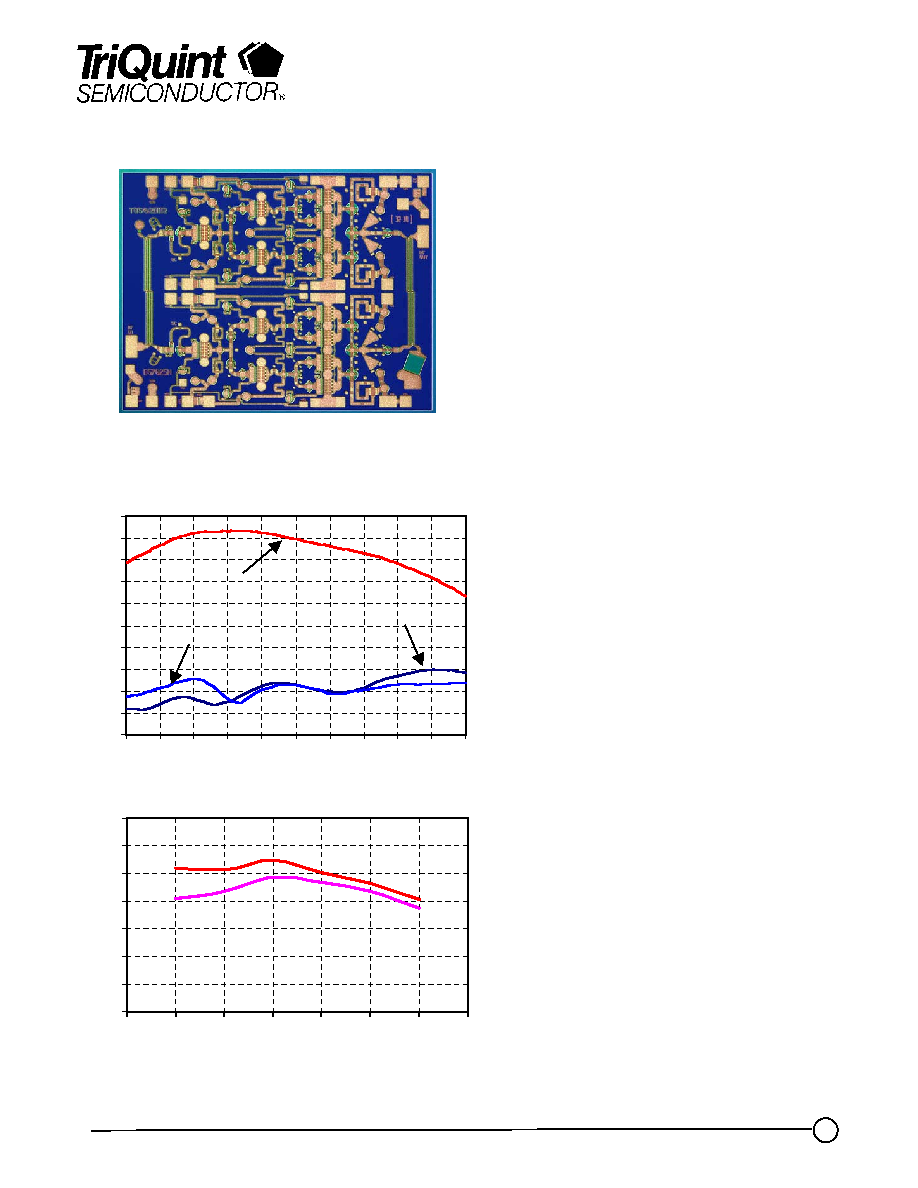
-25
-20
-15
-10
-5
0
5
10
15
20
25
25
26
27
28
29
30
31
32
33
34
35
Frequency (GHz)
Ga
i
n
(
d
B)
27 - 32 GHz 2W Balanced Power Amplifier TGA4513-EPU
Key Features
�
27 - 32 GHz Bandwidth
�
> 32 dBm P1dB
�
33 dBm Psat
�
20 dB Nominal Gain
�
IMR3 is 37 dBc @ 18 dBm SCL
�
14 dB Nominal Return Loss
�
Bias: 6 V, 840 mA
�
0.25 um 3MI mmW pHEMT Technology
�
Chip Dimensions: 2.8 x 2.2 x 0.1 mm
(0.110 x 0.087 x 0.004) in
Primary Applications
�
Point to Point Radio
�
Point to Multi Point Radio
�
LMDS
�
Satellite Ground Terminal
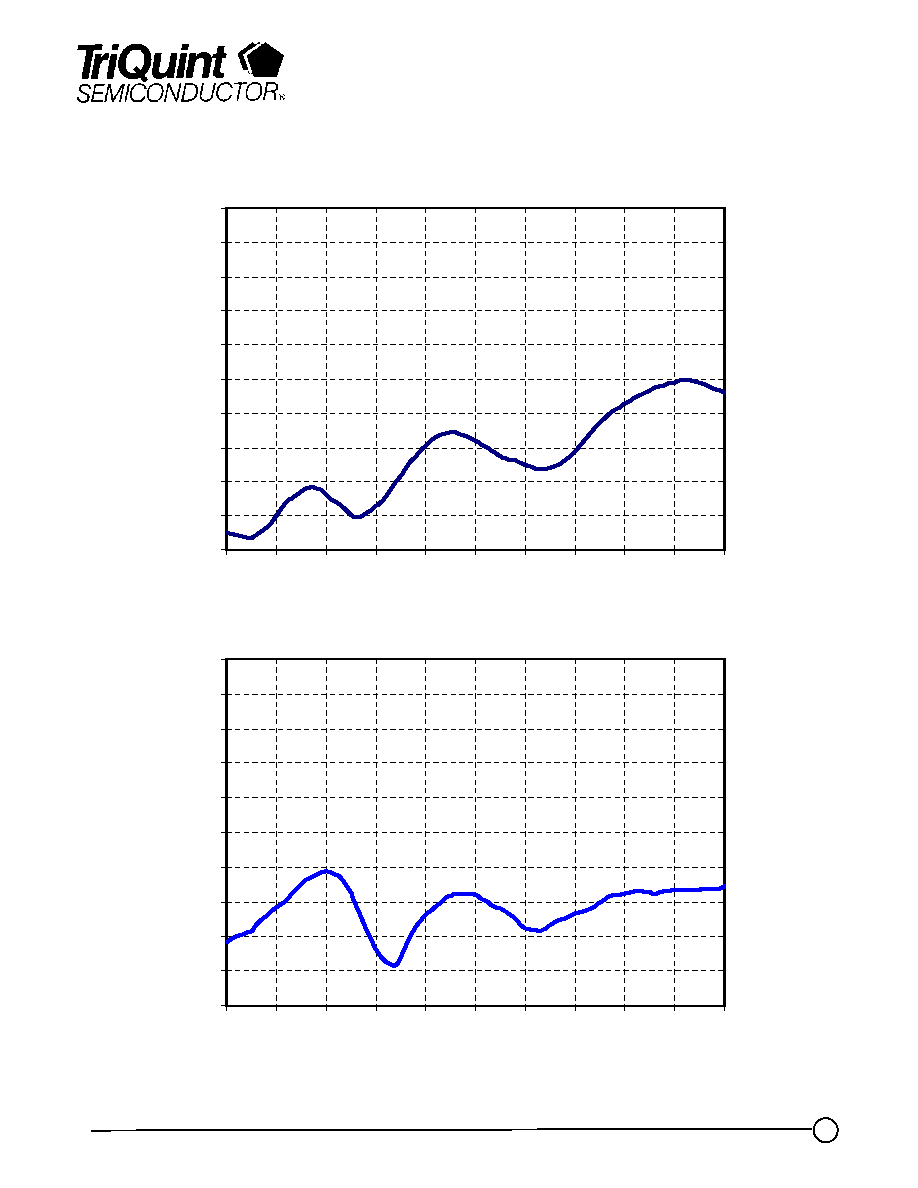
Preliminary Measured Data
Bias Conditions: Vd = 6 V, Id = 840 mA
ORL
IRL
Gain
28
29
30
31
32
33
34
35
26
27
28
29
30
31
32
33
Frequency (GHz)
Po
u
t
(
d
B
m
)
P1dB
Psat
TriQuint Semiconductor Texas: Phone (972)994-8465 Fax (972)994 8504 Web: www.triquint.com
Advance Product Information
Jan 27, 2003
2
Note: Devices designated as EPU are typically early in their characterization process prior to finalizing all electrical and process
specifications. Specifications are subject to change without notice
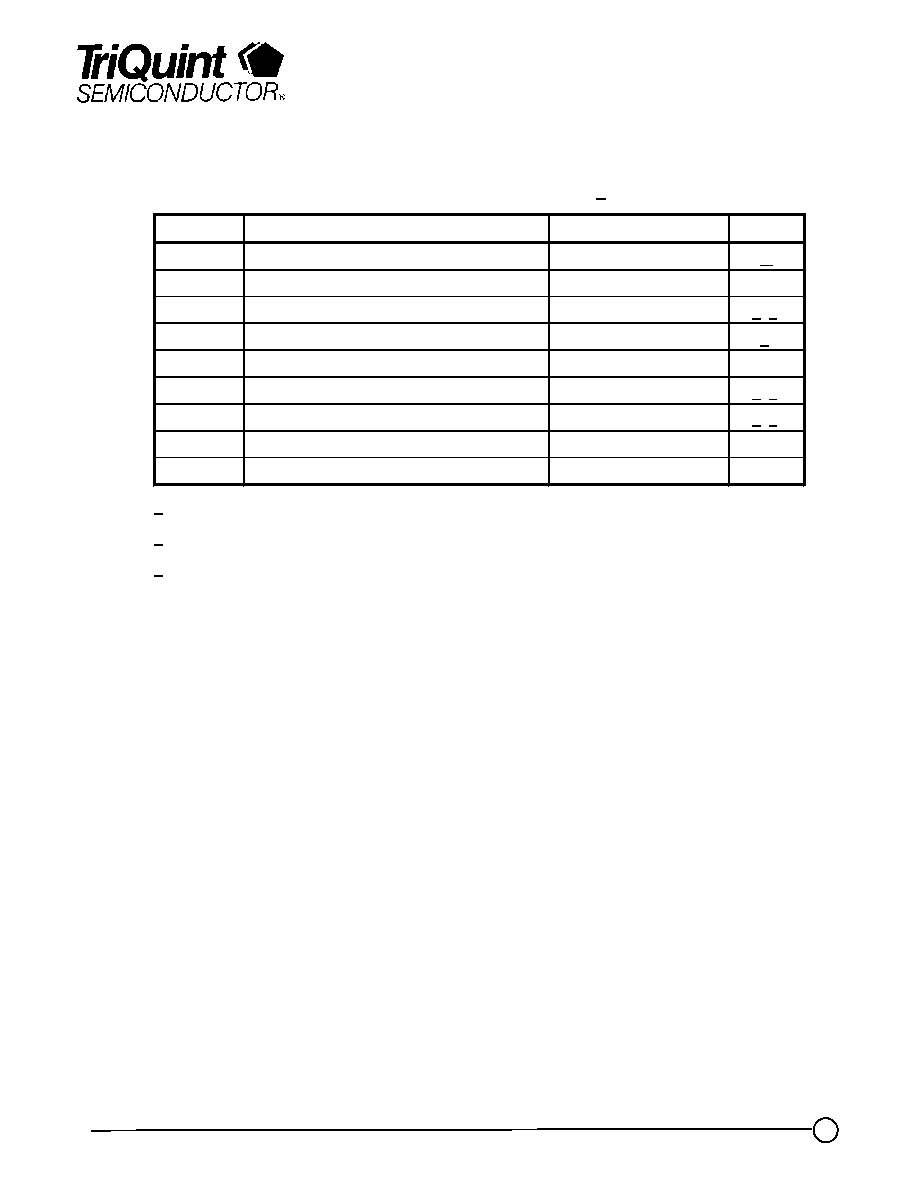
TABLE I
MAXIMUM RATINGS 1/
SYMBOL
PARAMETER
VALUE
NOTES
V
+
Positive Supply Voltage
6 V
2/
V
-
Negative Supply Voltage Range
-5 TO 0 V
I
+
Positive Supply Current
1.86 A
2/ 3/
�I
G
�
Gate Supply Current
70 mA
3/
P
IN
Input Continuous Wave Power
22 dBm
P
D
Power Dissipation
TBD
2/ 4/
T
CH
Operating Channel Temperature
150
0
C
5/ 6/
T
M
Mounting Temperature (30 Seconds)
320
0
C
T
STG
Storage Temperature
-65 to 150
0
C
1/
These ratings represent the maximum operable values for this device.
2/
Combinations of supply voltage, supply current, input power, and output power shall not exceed P
D
.
3/
Total current for the entire MMIC.
4/
When operated at this bias condition with a base plate temperature of TBD, the median life is
reduced from TBD to TBD hrs.
5/
Operating channel temperature will directly affect the device median time to failure (MTTF). For
maximum life, it is recommended that the channel (junction) temperatures be maintained at the
lowest possible levels.
6/
These ratings apply to each individual FET.
TGA4513-EPU
TriQuint Semiconductor Texas: Phone (972)994-8465 Fax (972)994 8504 Web: www.triquint.com
Advance Product Information
Jan 27, 2003
3
Note: Devices designated as EPU are typically early in their characterization process prior to finalizing all electrical and process
specifications. Specifications are subject to change without notice
TABLE III
ELECTRICAL CHARACTERISTICS
(Ta = 25
0
C, Nominal)
TGA4513-EPU
PARAMETER
TYPICAL
UNITS
Drain Operating
6
V
Quiescent Current
840
mA
Small Signal Gain, S21
20
dB
Input Return Loss, S11
14
dB
Output Return Loss, S22
14
dB
Reverse Isolation, S12
-40
dB
Output Power @ 1 dB Compression Gain, P1dB
> 32
dBm
Power @ saturated, Psat
33
dBm
IMR3 @ 18 dBm SCL
37
dBc
TABLE II
DC PROBE TESTS
(T
A
= 25
�C Nominal)
SYMBOL
PARAMETER
MINIMUM
MAXIMUM
VALUE
I
DSS1
Saturated Drain Current
60
282
V
G
M1
Transconductance
132
318
mS
V
BVGS1
Breakdown Voltage gate-source
-30
-8
V
V
BVGD1
Breakdown Voltage gate-drain
-30
-11
V
V
P1,8
Pinch-off Voltage
-1.5
-0.5
V
Q1 is 600 um FET
TriQuint Semiconductor Texas: Phone (972)994-8465 Fax (972)994 8504 Web: www.triquint.com
Advance Product Information
Jan 27, 2003
4
Note: Devices designated as EPU are typically early in their characterization process prior to finalizing all electrical and process
specifications. Specifications are subject to change without notice
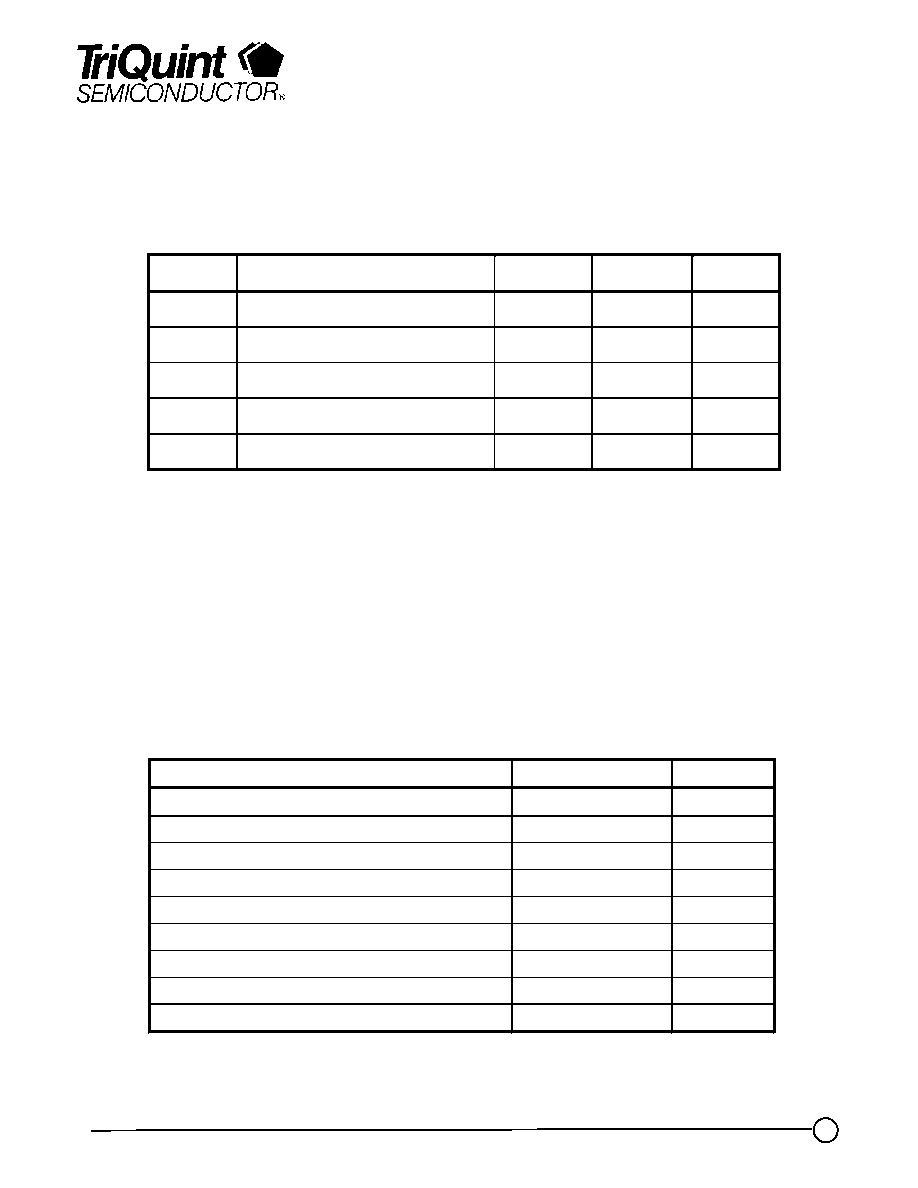
0
2
4
6
8
10
12
14
16
18
20
22
24
26
25
26
27
28
29
30
31
32
33
34
35
Frequency (GHz)
Ga
in
(
d
B
)
TGA4513-EPU
Preliminary Measured Data
Bias Conditions: Vd = 6 V, Id = 840 mA
-
40
0
C
+
70
0
C
Bias Conditions: Vd = 6 V, Id = 40 mA
+
25
0
C
28
29
30
31
32
33
34
35
26
27
28
29
30
31
32
33
Frequency (GHz)
P1
d
B
(
d
B
m
)
Psat
P1dB
TriQuint Semiconductor Texas: Phone (972)994-8465 Fax (972)994 8504 Web: www.triquint.com
Advance Product Information
Jan 27, 2003
5
Note: Devices designated as EPU are typically early in their characterization process prior to finalizing all electrical and process
specifications. Specifications are subject to change without notice
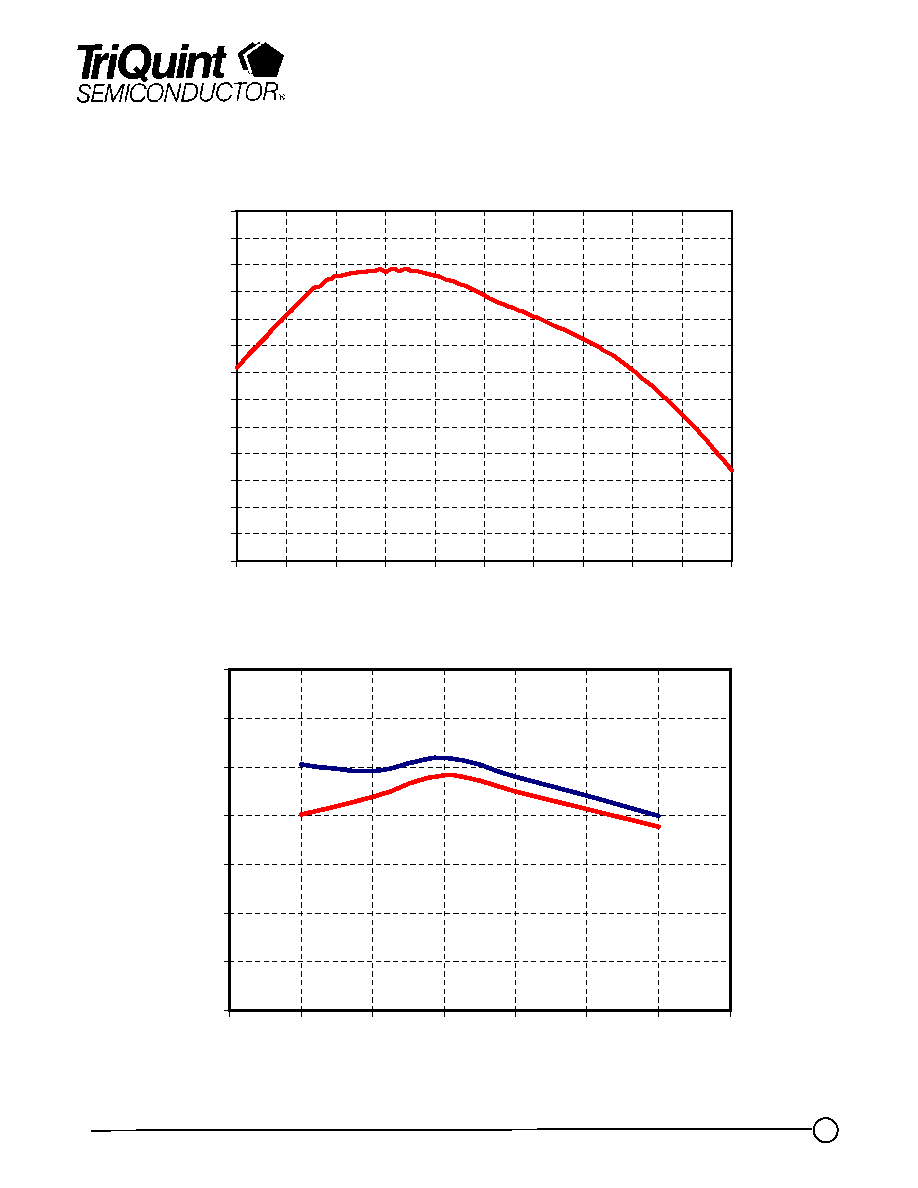
-20
-18
-16
-14
-12
-10
-8
-6
-4
-2
0
25
26
27
28
29
30
31
32
33
34
35
Frequency (GHz)
O
u
tpu
t
R
e
tur
n
L
o
s
s
(
d
B
)
-20
-18
-16
-14
-12
-10
-8
-6
-4
-2
0
25
26
27
28
29
30
31
32
33
34
35
Frequency (GHz)
I
npu
t
R
e
t
u
r
n
Los
s
(
d
B
)
TGA4513-EPU
Preliminary Measured Data
Bias Conditions: Vd = 6 V, Id = 840 mA
Document Outline