 | –≠–ª–µ–∫—Ç—Ä–æ–Ω–Ω—ã–π –∫–æ–º–ø–æ–Ω–µ–Ω—Ç: TGA4516 | –°–∫–∞—á–∞—Ç—å:  PDF PDF  ZIP ZIP |

TriQuint Semiconductor Texas: Phone (972)994-8465 Fax (972)994 8504 Email: Info-mmw@tqs.com Web: www.triquint.com
Advance Product Information
December 2, 2004
1
Ka-Band 2W Power Amplifier TGA4516
Key Features
∑
30 - 40 GHz Bandwidth
∑
> 33 dBm Nominal Psat @ Pin = 20dBm
∑
18 dB Nominal Gain
∑
Bias: 6 V, 1050 mA Idq
(1.9A under RF Drive)
∑
0.15 um 3MI MMW pHEMT Technology
∑
Chip Dimensions: 2.79 x 2.315 x 0.1 mm
(0.110 x 0.091 x 0.004) in
Primary Applications
∑
Military Radar Systems
∑
Ka-Band Sat-Com
∑
Point to Point Radio
Preliminary Fixtured Data
V
D
= 6V, I
D
= 1050mA
-35
-30
-25
-20
-15
-10
-5
0
5
10
15
20
25
30
32
34
36
38
40
Frequency (GHz)
S-Parameters (dB)
S21
S22
S11
Pout @ Pin =20dBm
30
31
32
33
34
35
30
32
34
36
38
40
Frequency (GHz)
Pout (dBm)
Product Description
The TriQuint TGA4516 is a High Power MMIC
Amplifier for Ka-band applications. The part
is designed using TriQuint's 0.15um power
pHEMT process. The small chip size is
achieved by utilizing TriQuint's 3 metal layer
interconnect (3MI) design technology that
allows compaction of the design over
competing products.
The TGA4516 provides >33 dBm saturated
output power, and has typical gain of 18 dB at
a bias of 6V and 1050mA (Idq). The current
rises to 1.9A under RF drive.
This HPA is ideally suited for many
applications such as Military Radar Systems,
Ka-band Sat-Com, and Point-to-Point
Radios.
The TGA4516 is 100% DC and RF tested
on-wafer to ensure performance compliance.
Note: This Devices is early in the characterization process prior to finalizing all electrical specifications. Specifications are subject to
change without notice.
TriQuint Semiconductor Texas: Phone (972)994-8465 Fax (972)994 8504 Email: Info-mmw@tqs.com Web: www.triquint.com
Advance Product Information
December 2, 2004
2
SYMBOL
PARAMETER
VALUE
NOTES
V
+
Positive Supply Voltage
8 V
2/
V
-
Negative Supply Voltage Range
-5 TO 0 V
I
+
Positive Supply Current
3 A
2/ 3/
I
G
Gate Supply Current
85 mA
3/
P
IN
Input Continuous Wave Power
267 mW
P
D
Power Dissipation
7.8 W
2/ 4/
T
CH
Operating Channel Temperature
150
o
C
5/ 6/
T
M
Mounting Temperature (30 Seconds)
320
o
C
T
S T G
Storage Temperature
-65 to 150
o
C
1/
These ratings represent the maximum operable values for this device.
2/
Combinations of supply voltage, supply current, input power, and output power shall not
exceed P
D
.
3/
Total current for the entire MMIC.
4/
When operated at this bias condition with a base plate temperature of 70
o
C, the median life
is 1E6 hrs.
5/
Junction operating temperature will directly affect the device median time to failure (MTTF).
For maximum life, it is recommended that junction temperatures be maintained at the lowest
possible levels.
6/
These ratings apply to each individual FET.
TGA4516
TABLE I
MAXIMUM RATINGS 1/

TriQuint Semiconductor Texas: Phone (972)994-8465 Fax (972)994 8504 Email: Info-mmw@tqs.com Web: www.triquint.com
Advance Product Information
December 2, 2004
3
TABLE III
ELECTRICAL CHARACTERISTICS
(Ta = 25
O
C, Nominal)
PARAMETER
TYPICAL
UNITS
Drain Operating
6
V
Quiescent Current
1050
mA
Frequency Range
30 - 40
GHz
Small Signal Gain, S21
18
dB
Input Return Loss, S11
10
dB
Output Return Loss, S22
7
dB
Power @ saturated, Psat
33
dBm
Q1- Q4 are 400 um FETs, Q5 is 2560 um FET, Q6 is 4160 um FET
SYMBOL
PARAMETER
MIN.
MAX.
UNITS
I
DSS,Q1
Saturated Drain Current
80
240
mA
V
BVGS,Q1
Breakdown Voltage Gate-Source
-18
-8
V
V
BVGD,Q1-Q6
Breakdown Voltage Gate-Drain
-18
-11
V
V
P,Q1-Q6
Pinch_off Voltage
-1.5
-0.5
V
TGA4516
TABLE II
DC PROBE TESTS
(Ta = 25
O
C, Nominal)
Parameter
Test Conditions
T
ch
(
o
C)
R
JC
(
o
C/W)
T
M
(HRS)
R
JC
Thermal Resistance
(channel to backside of carrier)
Vd = 6 V
Id = 1700 mA
Freq = 35 GHz
Pdiss = 7.8 W
150
10.2
1E+6
TABLE IV
THERMAL INFORMATION
Note: Assumes eutectic attach using 1.5 mil 80/20 AuSn mounted to a 20 mil CuMo Carrier at 70
∞
C baseplate temperature.
Worst case is at saturated output power when DC power consumption rises to 10.6 W with 2.3 W RF power delivered to load.
Power dissipated is 8.2 W and the temperature rise in the channel is 84
∞
C. Baseplate temperature must be reduced to 66
∞
C to
remain below the 150
∞
C maximum channel temperature.

TriQuint Semiconductor Texas: Phone (972)994-8465 Fax (972)994 8504 Email: Info-mmw@tqs.com Web: www.triquint.com
Advance Product Information
December 2, 2004
4
Fixtured Performance
TGA4516 Pout @ Pin =20dBm
Vds=6V, Idq=1050mA
25
26
27
28
29
30
31
32
33
34
35
28
3 0
32
34
3 6
38
40
42
Frequency (GHz)
Pout (dBm)
Pin=20dBm
TGA4516
Vds=6V, Idq=1050mA
-40
-35
-30
-25
-20
-15
-10
-5
0
5
10
15
20
25
28
30
32
34
36
38
40
42
Frequency (GHz)
S-Parameters (dB)
S11
S22
S21
TriQuint Semiconductor Texas: Phone (972)994-8465 Fax (972)994 8504 Email: Info-mmw@tqs.com Web: www.triquint.com
Advance Product Information
December 2, 2004
5
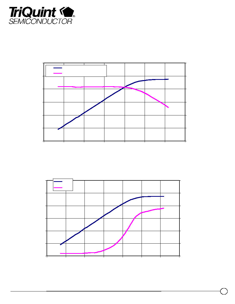
Fixtured Performance
TGA4516 Pout vs. Pin
freq=35GHz, Vds=6V, Idq=1050mA
10
15
20
25
30
35
40
-10
-5
0
5
10
15
20
25
Pin (dBm)
Pout (dBm)
0
5
10
15
20
25
30
Gain (dB)
Pout
Large Signal Gain
TGA4516
TGA4516 Ids vs. Pin
freq=35GHz, Vds=6V, Idq=1050mA
10
15
20
25
30
35
40
-10
-5
0
5
10
15
20
25
Pin (dBm)
Pout (dBm)
1000
1200
1400
1600
1800
2000
2200
IDS (mA)
Pout
Ids