 | ÐлекÑÑоннÑй компоненÑ: TGA9092 | СкаÑаÑÑ:  PDF PDF  ZIP ZIP |
Äîêóìåíòàöèÿ è îïèñàíèÿ www.docs.chipfind.ru
TriQuint Semiconductor Texas : Phone (972)994 8465 Fax (972)994 5804 Web: www.triquint.com
Advance Product Information
1
6 - 18 GHz High Power Amplifier TGA9092-EPU
Key Features and Performance
·
Dual Channel Power Amplifier
·
0.25um pHEMT Technology
·
6-18 GHz Frequency Range
·
2.8 W/Channel Midband Pout
·
5.6 W Pout Combined
·
25 dB Nominal Gain
·
Balanced In/Out for Low VSWR
·
8V @ 1.2A per Channel Bias
Primary Applications
·
X-Ku band Power
·
Point-to-Point Radio
·
VSAT
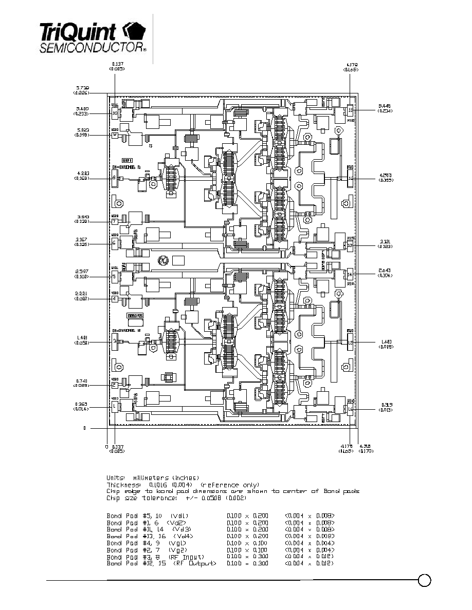
Chip Dimensions 4.32mm x 5.64mm x 0.100mm
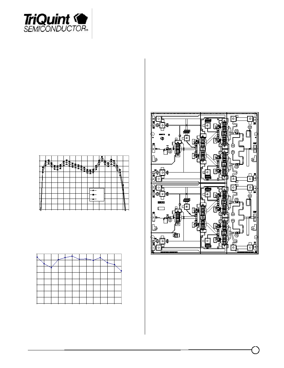
Typical Measured Small Signal Gain
Typical Measured Pout (RF Probe)
TGA9092-EPU Average Pout
RF Probe Data
20.00
22.00
24.00
26.00
28.00
30.00
32.00
34.00
36.00
6
7
8
9
10
11
12
13
14
15
16
17
18
Frequency (GHz)
Pout (dBm)
TGA9092-EPU Measured S21 Data
10.00
12.00
14.00
16.00
18.00
20.00
22.00
24.00
26.00
28.00
30.00
5
6
7
8
9
10
11
12
13
14
15
16
17
18
19
20
Frequency (GHz)
Gain (dB)
Mean
+1std
-1std
Note: Devices designated as EPU are typically early in their characterization process prior to finalizing all electrical and process
specifications. Specifications are subject to change without notice.
TriQuint Semiconductor Texas : Phone (972)994 8465 Fax (972)994 5804 Web: www.triquint.com
Advance Product Information
Table I
RECOMMENDED MAXIMUM RATINGS
Symbol
Parameter
Value
Notes
V
+
Positive Supply Voltage
9 V
I
+
Positive Supply Current
3.5 A
3/
P
D
Power Dissipation
25 Watts
P
IN
Input Continuous Wave Power
25 dBm
T
CH
Operating Channel Temperature
150
°
C
1/, 2/
T
M
Mounting Temperature (30 seconds)
320
°
C
T
STG
Storage Temperature
-65
°
C to 150
°
C
1/
These ratings apply to each individual FET
2/
Junction operating temperature will directly affect the device mean time to failure
(MTTF). For maximum life it is recommended that junction temperatures be
maintained at the lowest possible levels.
3/
Total current for both channels
Table II
DC PROBE TESTS
(T
A
= 25
°
C
±
5
°
C)
Symbol
Parameter
Minimum Maximum
Value
V
P1-14
Pinch-off Voltage
-1.5
-0.5
V
BV
GS1
Breakdown Voltage gate-source
-30
-8
V
BV
GD1-3
Breakdown Voltage gate-drain
-30
-8
V
Table III
ON-WAFER RF PROBE CHARACTERISTICS
(T
A
= 25
°
C
±
5
°
C)
Symbol Parameter
Test Condition
Vd=8V, Id=800mA
Limit
Min Nom Max
Units
G
p
Small-signal
Power Gain
F = 6 to 18 GHz
21
25
31
dB
P
3dB
Output Power
@ 3dB gain
compression
F = 6 to 9 GHz
F = 10 to 17 GHz
F = 18 Ghz
30
33
30
32
34
33
-
-
-
dBm
PAE
Power Added
Efficiency
F = 6 to 18 GHz
12
25
-
%
Note: RF probe data taken at 1GHz steps
Note: Devices designated as EPU are typically early in their characterization process prior to finalizing all electrical and process
specifications. Specifications are subject to change without notice.
TriQuint Semiconductor Texas : Phone (972)994 8465 Fax (972)994 5804 Web: www.triquint.com
Advance Product Information
TriQuint Semiconductor Texas : Phone (972)994 8465 Fax (972)994 5804 Web: www.triquint.com
Advance Product Information
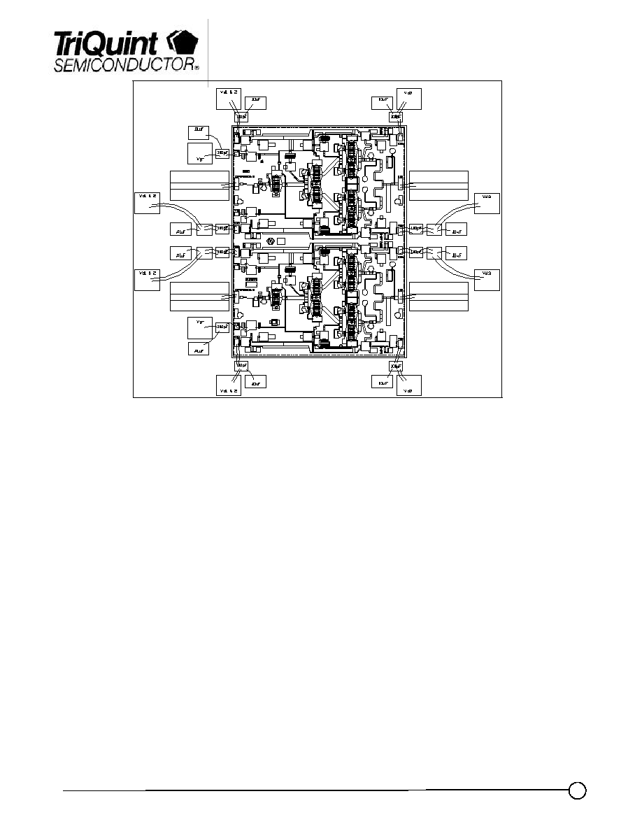
Chip Assembly and Bonding Diagram
Reflow process assembly notes:
·
AuSn (80/20) solder with limited exposure to temperatures at or above 300
C
·
alloy station or conveyor furnace with reducing atmosphere
·
no fluxes should be utilized
·
coefficient of thermal expansion matching is critical for long-term reliability
·
storage in dry nitrogen atmosphere
Component placement and adhesive attachment assembly notes:
·
vacuum pencils and/or vacuum collets preferred method of pick up
·
avoidance of air bridges during placement
·
force impact critical during auto placement
·
organic attachment can be used in low-power applications
·
curing should be done in a convection oven; proper exhaust is a safety concern
·
microwave or radiant curing should not be used because of differential heating
·
coefficient of thermal expansion matching is critical
Interconnect process assembly notes:
·
thermosonic ball bonding is the preferred interconnect technique
·
force, time, and ultrasonics are critical parameters
·
aluminum wire should not be used
·
discrete FET devices with small pad sizes should be bonded with 0.0007-inch wire
·
maximum stage temperature: 200
C
GaAs MMIC devices are susceptible to damage from Electrostatic Discharge. Proper precautions should
be observed during handling, assembly and test.