 | –≠–ª–µ–∫—Ç—Ä–æ–Ω–Ω—ã–π –∫–æ–º–ø–æ–Ω–µ–Ω—Ç: TGF4250 | –°–∫–∞—á–∞—Ç—å:  PDF PDF  ZIP ZIP |
ete HFET
4250
TGF4250-EEU
4.8 mm Discr
q
4800 µm x 0.5 µm HFET
q
Nominal Pout of 34- dBm at 8.5- GHz
q
Nominal Gain of 8. 5- dB at 8.5- GHz
q
Nominal PAE of 53% at 8.5 - GHz
q
Suitable for high reliability applications
q
0,572 x 1,334 x 0,102 mm (0.023 x 0.053 x 0.004 in.)
The TriQuint TGF4250-EEU is a single gate 4.8 mm discrete GaAs Heterostructure Field
Ef fect Transistor (HFET) designed for high ef ficiency power applications up to 10. 5- GHz in Class A and
Class AB operation. Typical performance at 2- GHz is 34 - dBm power output, 13 - dB gain, and 63% PAE.
Bond pad and backside metalization is gold plated for compat ibility with eutectic alloy attach
methods as well as thermocompr ession and ther mosonic wire-bonding processes. The TGF4250-EEU
is readily assembled using automatic equipment.
PHOTO ENLARGEMENT
DESCRIPTION
TriQuint Semiconductor, Inc.
∑ Texas Facilities
∑ (972) 995-8465
∑ www.triquint.com
T R I Q U I N T
S E M I C O N D U C T O R , I N C .
TGF4250-EEU
2
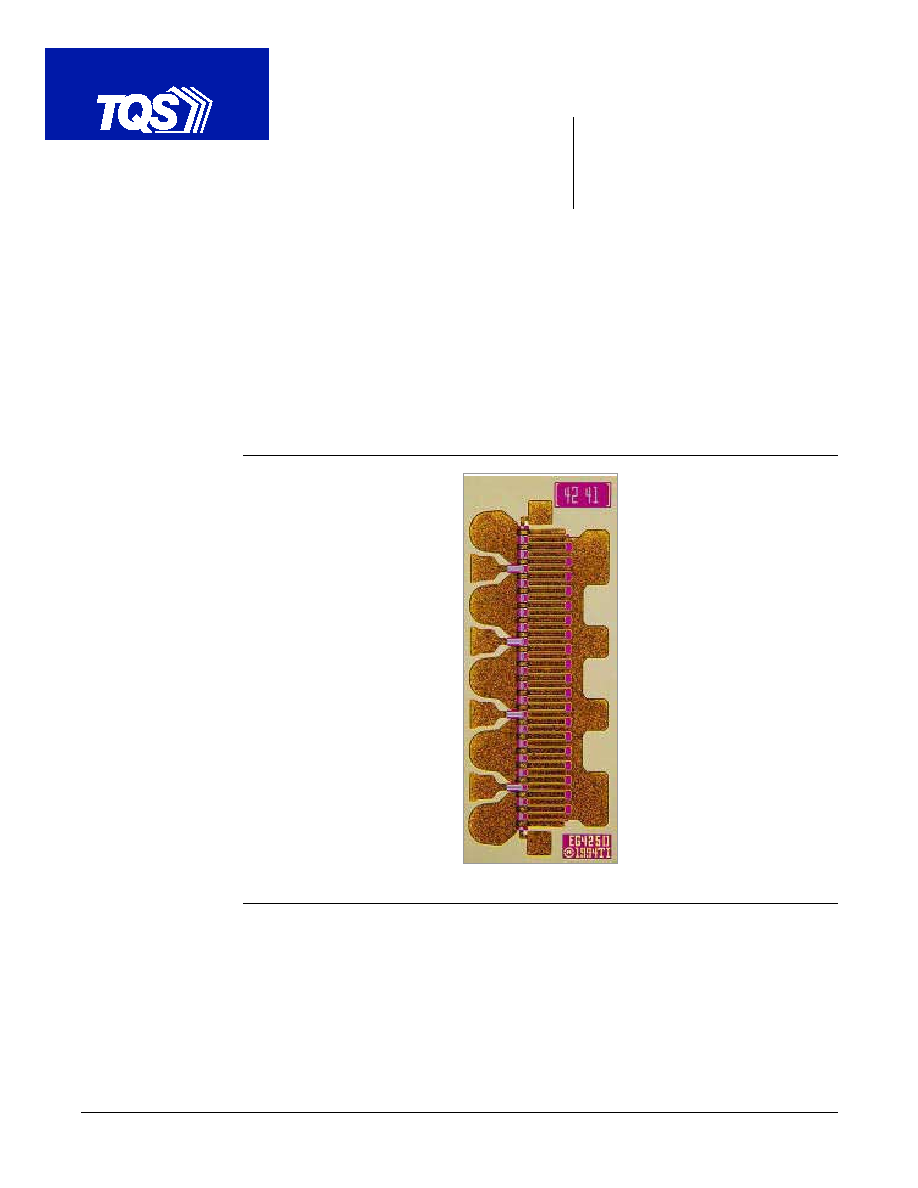
EXAMPLE OF
DC I-V CURVES
p
0
0.1
0.2
0.3
0.4
0.5
0.6
0.7
0.8
0.9
1
1.1
0
1
2
3
4
5
6
7
8
9
10
Drain Voltage (V)
Drain Current (A)
V
G
= 0.0 to -2.25 V
(0.25 V steps)
T
A
=65∞C
OUTPUT POWER
VS. INPUT POWER
20
22
24
26
28
30
32
34
36
10
12
14
16
18
20
22
24
26
28
Input Power (dBm)
Output Power (dBm)
F =8.5 GHz
V
D
=8.0 V
I
Q
=200 mA
T
A
=25∞C
POWER ADDED
EFFICIENCY VS.
INPUT POWER
0
5
10
15
20
25
30
35
40
45
50
55
10
12
14
16
18
20
22
24
26
28
Input Power (dBm)
PAE (%)
F =8.5 GHz
V
D
=8.0 V
I
Q
=200 mA
T
A
=25∞C
* I
Q
is defined as the drain current before application of RF signal at the input.
*
TriQuint Semiconductor, Inc.
∑ Texas Facilities
∑ (972) 995-8465
∑ www.triquint.com

TGF4250-EEU
3
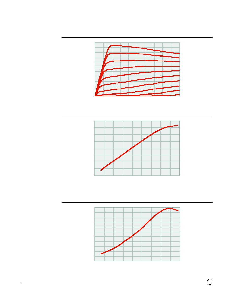
GAIN VS.
INPUT POWER
7
8
9
10
11
10
12
14
16
18
20
22
24
26
28
Input Power (dBm)
Gain (dB)
F =8.5GHz
V
D
=8.0V
I
Q
=200 mA
T
A
=25∞C
DRAIN CURRENT
VS. INPUT POWER
0.2
0.25
0.3
0.35
0.4
0.45
0.5
0.55
0.6
10
12
14
16
18
20
22
24
26
28
Input Power (dBm)
Drain Current (A)
F =8.5GHz
V
D
=8.0V
I
Q
=200 mA
T
A
=25∞C
ABSOLUTE MAXIMUM
RATINGS
Drain - to- source voltage, V
DS
................................................................................................................ 12 V
Gate - to- source voltage, V
GS
........................................................................................................ -5 V to 0 V
Mounting temperatur e (30 sec), T
M
.................................................................................................. 320 C
Storage temperature range, T
STG
............................................................................................ - 65 to 200 C
Power dissipation, P
D
..................................................................................
Operating channel temperature, T
CH
............................................................
(see ther mal data on next page)
(see ther mal data on next page)
Ratings over operating channel temperature (unless otherwise noted)
Stresses beyond those listed under "Absolute Maximum Ratings" may cause permanent damage to the device.
These are stress ratings only, and functional operation of the device at these or any other conditions beyond
those indicated under "RF and DC Characteristics" is not implied. Exposure to absolute maximum rated conditions
for extended periods may affect device reliability.
TriQuint Semiconductor, Inc.
∑ Texas Facilities
∑ (972) 995-8465
∑ www.triquint.com
TGF4250-EEU
4
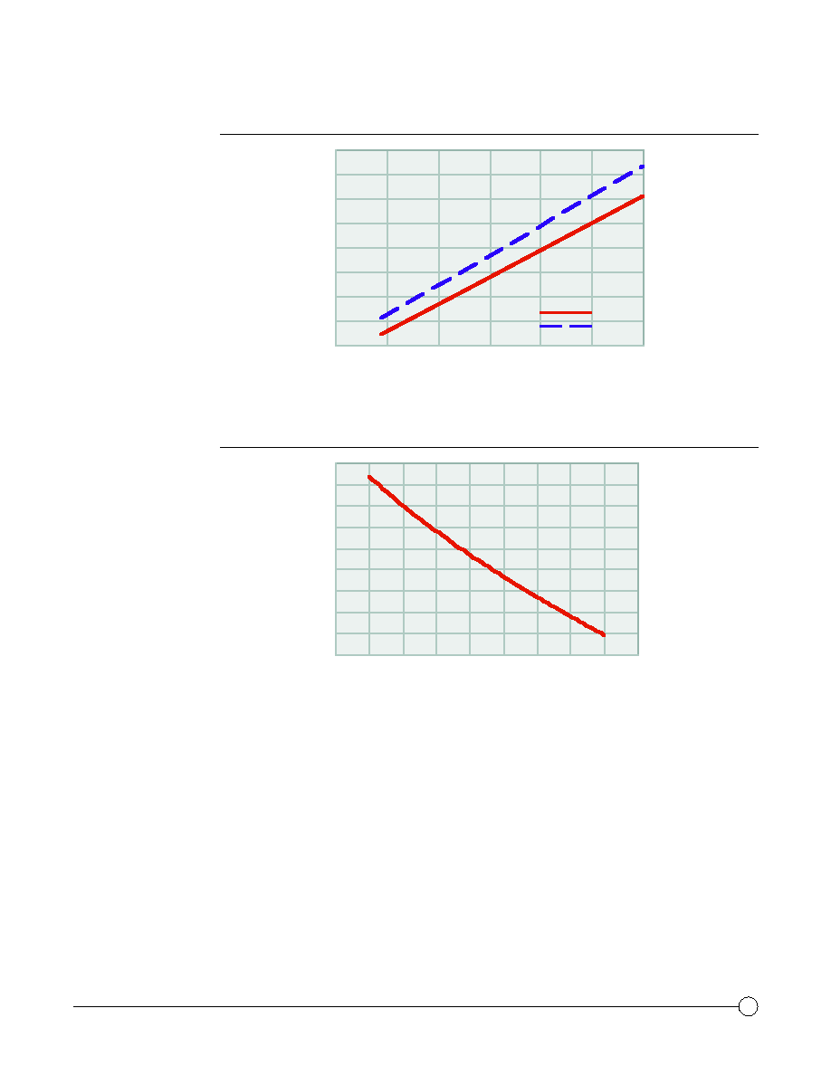
HFET CHANNEL
TEMPERATURE VS.
MEDIAN LIFE
100
125
150
175
200
225
250
275
300
325
1
2
3
4
5
6
7
8
9
10
Median Life (10^X Hours)
Channel Temperature (∞
C
)
11415 years
PREDICTED CHANNEL
TEMPERATURE VS.
CARRIER BASE
TEMPERATURE
at 2.04 W and 4.08 W
dissipated power
p
-50
0
50
100
150
200
250
300
350
-100
-50
0
50
100
150
200
Channel Temperature (∞
C
)
2.04 W
4.08 W
Carrier Base T emperatur e (∞C)
38 µm AuSn solder attach to 0.5 mm CuMo Carrier.
Median Life (10^ x Hours)
TriQuint Semiconductor, Inc.
∑ Texas Facilities
∑ (972) 995-8465
∑ www.triquint.com

TGF4250-EEU
5
RF AND DC
CHARACTERISTICS
LINEAR MODEL
PARAMETER
MIN
NOMINAL
MAX
UNIT
Pout
Output Power
33
34
-
dBm
G
P
Power Gain
7
8.5
-
dB
P A E
Power Added Efficiency
47
53
-
%
I
DSS
Drain Saturation Current
816
1176
1536
mA
G
M
Transconductance
576
792
1008
mS
V
P
Pinch Off Voltage
-2.7
-1.85
-1
V
BV
GS
Breakdown Voltage Gate-Source
- 30
- 22
- 17
V
BV
GD
Breakdown Voltage Gate-Drain
- 30
- 22
- 17
V
Pout, Gain, and P AE: Measured at 8.5- GHz, drain voltage of 8.0 V . Gate voltage is adjusted to achieve
quiescent current of approximately 20% I
DSS
with no RF signal applied. The source is grounded. Input power
between 25 and 26- dBm.
I
DSS
: Saturated drain- source current. Sear ch for the maximum I
DS
at V
GS
= 0.0 V, and V
DS
swept between 0.5 V
to 3.5 V. Note that the drain voltage at which I
DSS
is located and r ecorded as V
DSP
.
G
M
: Transconductance. (I
DSS
- I
DS1
)/
I
V
G
1
I
. I
DS1
measured at V
G1
= - 0.25 V using the knee sear ch technique;
V
DS
swept between 0.5 V and V
DSP
to search for maximum I
DS1
.
V
P
: Pinch off voltage. V
GS
for I
DS
= 0.5 mA/mm of gate width. V
DS
fixed at 2.0 V, V
GS
swept to bring I
DS
to
0.5 mA/mm. Sweep will stop if V
P
current not found beyond 0.5 V of the minimum V
P
specification.
BV
GS
: Breakdown voltage, gate to source. I
BD
= 1.0 mA/mm of gate width. Source fixed at ground, drain not
connected (floating). When 1.0mA/mm drawn at gate, V
GS
measured as BV
GS
.
BV
GD
: Breakdown voltage, gate to drain. I
BD
= 1.0 mA/mm of gate width. Drain fixed at ground, source not
connected (floating). When 1.0 mA/mm drawn at the gate, V
GD
measured as BV
GD
.
G
R
G
R
GS
C
GS
R
DG
C
DG
V
CCS
L
D
R
D
D
C
DS
R
DS
R
2
R
1
R
S
L
S
R
I
L
G
FET Elements
L
G
= 0.010525 nH
R
G
= 0.21075
R
GS
= 20425
R
I
= 0.3025
C
GS
= 4.84 pF
C
DG
= 0.4015 pF
R
DG
= 51000
R
S
= 0.1
L
S
= 0.011 nH
R
DS
= 24.5025
C
DS
= 1.013 pF
R
D
= 0.165
L
D
= 0.0055 nH
VCCS Parameters
M = 531.6 mS
A = 0
R1 = 1E19
R2 = 1E19
F = 0
T = 5.49 pS
V
DS
= 8.0 V and 30% I
DSS
at T = 25∞C
TriQuint Semiconductor, Inc.
∑ Texas Facilities
∑ (972) 995-8465
∑ www.triquint.com