
1
SWITCHING
PRODUCTS
For additional information and latest specifications, see our website: www.triquint.com
T
R
I Q
U
I
N
T
S E M I C O N D U C T O R , I N C .
VTT
IN0
NIN0
IADD
OADD
LOAD
CONFIG
2
2
CONTROL
4:1
4:1
4:1
4:1
VTT
IN1
NIN1
VTT
IN2
NIN2
VTT
IN3
NIN3
4
4
4
4
OUT0
NOUT0
+
-
OUT3
NOUT3
+
-
OUT2
NOUT2
+
-
OUT1
NOUT1
+
-
+
-
+
-
+
-
+
-
2 2 2 2
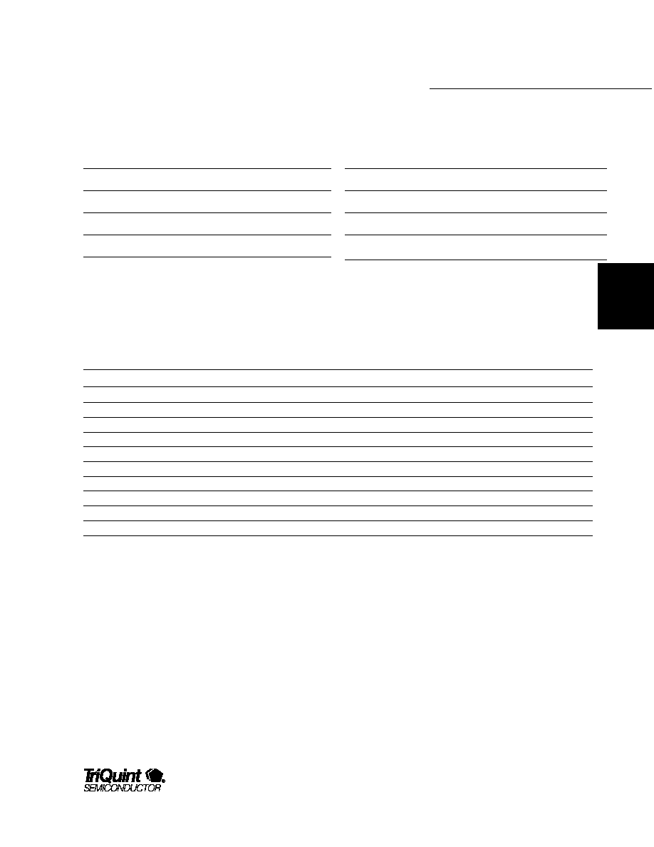
The TQ8004 is a non-blocking 4 X 4 digital crosspoint switch capable of
data rates greater than 2.7 Gigabits per second per port. Utilizing a fully
differential data path from input to output, the TQ8004 offers a high data
rate with exceptional fidelity. The symmetrical switching and noise
rejection characteristics inherent in differential logic result in low jitter, low
crosstalk and minimum signal skew. The TQ8004 is ideal for high speed
data switching applications, as well as high fidelity buffering or protection
switching.
The non-blocking architecture uses 4 fully independent 4:1 multiplexers,
allowing each input port to be independently programmed to any output
port.
TQ8004
2.7 Gbit/sec
3.3V 4x4 Digital
Crosspoint Switch
Features
� 2.7 Gb/s port data bandwidth
� Single 3.3V power supply
� Fully differential data path
� Non-blocking architecture
� Differential PECL I/O
TTL control inputs
� On-chip input termination
� Low jitter and channel to channel
signal skew
� Double configuration latches
� Small 28-pin TSSOP package
Applications
� Telecom/Datacom/Video
switching
� Fanout buffering
� Protection Switching

TQ8004
2
For additional information and latest specifications, see our website: www.triquint.com
Circuit Description
Data inputs
The 4 input channels are differential PECL compatible,
referenced to VDD = 3.3V power supply (LVPECL). All
LVPECL inputs have on-chip 50 Ohm termination to
VTT.
For AC coupled designs an internal bias generator can
be used to supply the VTT voltage. An on-chip voltage
divider generates the VTT voltage at VDD-1.3V with an
impedance of 800 Ohms. Due to the high impedance of
the internal VTT source it is suited only for AC coupled
input schemes.
For DC coupled designs VTT needs to be externally
supplied, nominally at VDD-2.0V for LVPECL systems.
Note that the external source needs to be able to sink
current.
If any inputs are unused, terminate one side of any
unused input pair to GND through a 500 Ohm or
smaller resistor. This will prevent unwanted
oscillations.
Data outputs
The 4 output channels are differential PECL and are
designed to be terminated through 50 Ohm to VDD-
2.0V. Unused outputs can be left unterminated.
Control inputs
The control inputs are TTL compatible. Unconnected
inputs will default to a logic HI level.
Switch configuration
The switch is configured by programming each output
to a specific input. Each of the 4 output channels have
two sets of program store latches. The first, or
program latch, stores a new input configuration prior
to application to the switch core. The second, or
configuration latch, stores the current input
configuration which is applied to the switch core. The
use of two sets of program storage latches allows for a
new set of input configurations to be loaded
simultaneously without disturbing the existing
configuration.
The address of the desired output is applied to
OADD(0:1). The input address is applied to IADD(0:1).
The input address defines which input port connects to
the selected output port. The new configuration is
loaded into the program latches by asserting the LOAD
signal high and is latched when LOAD is de-asserted.
The process is repeated for each new output port
configuration. Only the output ports which are to
receive a new input port configuration need to be
programmed in this manner. The new configurations
are not applied to the switch core at this time.
After all of the new configurations have been loaded
into the program latches, the CONFIGURE input is
asserted high and the data in the program latches is
loaded into the configuration latches. The data is
latched when CONFIGURE is de-asserted. Data integrity
is maintained on output ports not receiving a new
configuration
The switch core receives the new configuration
immediately following the assertion of CONFIGURE.
The integrity of the data on any re-configured output
port is unknown for a period
t
dcf
from the time
CONFIGURE is asserted.
The LOAD and CONFIGURE inputs can be asserted
simultaneously. In this mode, the new configuration
will be applied to the switch when LOAD is asserted.
TQ8004
3
SWITCHING
PRODUCTS
For additional information and latest specifications, see our website: www.triquint.com
Specifications
Table 1. Absolute Maximum Ratings
4
Parameter
Condition
Symbol
Minimum
Nominal
Maximum
Unit
Storage Temperature
T
store
�65
150
�C
Junction Temperature
T
CH
�65
150
�C
Case Temperature w/bias
(1)
T
C
0
100
�C
Supply Voltage
(2)
V
DD
0
5.5
V
Voltage to any input
(2)
V
in
�0.5
V
DD
+ 0.5
V
Voltage to any output
(2)
V
out
�0.5
V
DD
+ 0.5
V
Current to any LVTTL input
(2)
I
in
�1.0
1.0
mA
Current to any LVPECL input
(2)
I
in
�65
65
mA
Current from any output
(2)
I
out
40.0
mA
Power Dissipation of output
(3)
P
out
50.0
mW
Notes: 1. Tc is measured at case top.
2. All voltages are measured with respect to GND (0V) and are continuous.
3. Pout = (V
DD
� V
out
) x I
out
.
4. Absolute maximum ratings, as detailed in this table, are the ratings beyond which the device's performance may be impaired
and/or permanent damage to the device may occur.
Specifications subject to change without notice
Summary of the IADD(0:1) and OADD(0:1):
IADD1
IADD0
Input
0
0
IN0
0
1
IN1
1
0
IN2
1
1
IN3
OADD1
OADD0
Output
0
0
OUT0
0
1
OUT1
1
0
OUT2
1
1
OUT3

TQ8004
4
For additional information and latest specifications, see our website: www.triquint.com
Table 3. DC Characteristics--PECL I/O
3
Parameter
Condition
Symbol
Minimum
Nominal
Maximum
Unit
Input common mode voltage range
V
ICOM
V
DD
� 1500
--
V
DD
� 1100
mV
Input differential voltage (pk-pk)
(1)
V
IDIFF
600
--
2400
mV
Output common mode voltage range
V
OCOM
V
DD
-1500
--
V
DD
� 1100
mV
Output differential voltage (pk-pk)
(1,2)
V
ODIFF
1200
--
2400
mV
Input termination resistance
R
IN
50
Ohm
Input capacitance
C
IN
--
2.5
--
pF
Output capacitance
C
OUT
--
2.5
--
pF
ESD breakdown rating
V
ESD
1000
--
--
V
Table 4. DC Characteristics--TTL Inputs
3
Parameter
Condition
Symbol
Minimum
Nominal
Maximum
Unit
Input HIGH voltage
V
IH
2.0
--
V
DD
V
Input LOW voltage
V
IL
0
--
0.8
V
Input HIGH current
V
IH(MAX)
I
IH
--
--
200
uA
Input LOW current
V
IL(MIN)
I
IL
�400
�200
--
uA
Input capacitance
C
IN
--
2.5
--
pF
ESD breakdown rating
V
ESD
1000
--
--
V
Notes (Tables 3 and 4):
1. Differential Input Peak-Peak = 2| Vin - NVin |
2. R
LOAD
= 50 ohms to V
TT
= V
DD
� 2.0V.
3. Specifications apply over recommended operating ranges.
Table 2. Recommended Operating Conditions
3
Symbol
Parameter
Min
Typ
Max
Units
Notes
T
A
Operating Temperature
0
--
85
�C
1
V
DD
Supply Voltage
3.14
--
3.47
V
I
DD
Current Positive Supply
300
mA
V
TT
Load Termination Supply Voltage
V
DD
� 2.0
V
2
R
LOAD
Output Termination Load Resistance
50
2
JA
Thermal Resistance Junction to Ambient
40
�C/W
Notes: 1. Package thermal pad to be soldered to PCB.
2. The V
TT
and R
LOAD
combination is subject to maximum output current and power restrictions. Note that the value shown
is for DC coupled LVPECL I/O.
3. Functionality and/or adherence to electrical specifications is not implied when the device is subjected to conditions that exceed,
singularly or in combination, the operating range specified.
TQ8004
5
SWITCHING
PRODUCTS
For additional information and latest specifications, see our website: www.triquint.com
Table 5. AC Characteristics
Parameter
Condition
Symbol
Minimum
Nominal
Maximum
Unit
Maximum Data Rate/port
2.7
Gb/s
Minimum Input pulse width
(1)
T
pw
370
--
--
ps
Rise/Fall time 20-80%
T
r/f
--
--
150
ps
Channel Propagation Delay
(1)
T
pd
--
--
1.0
ns
Ch-to-Ch Prop. Delay Skew
(1)
T
skew
100
ps
Jitter (pk-pk)
(2)
T
jitter
--
25
--
ps
Notes: 1. Measured at crossing point of true and complement
2. Crossing of (On) � (NOn) measured with 2
23
� 1 PRBS, measured over extended time.
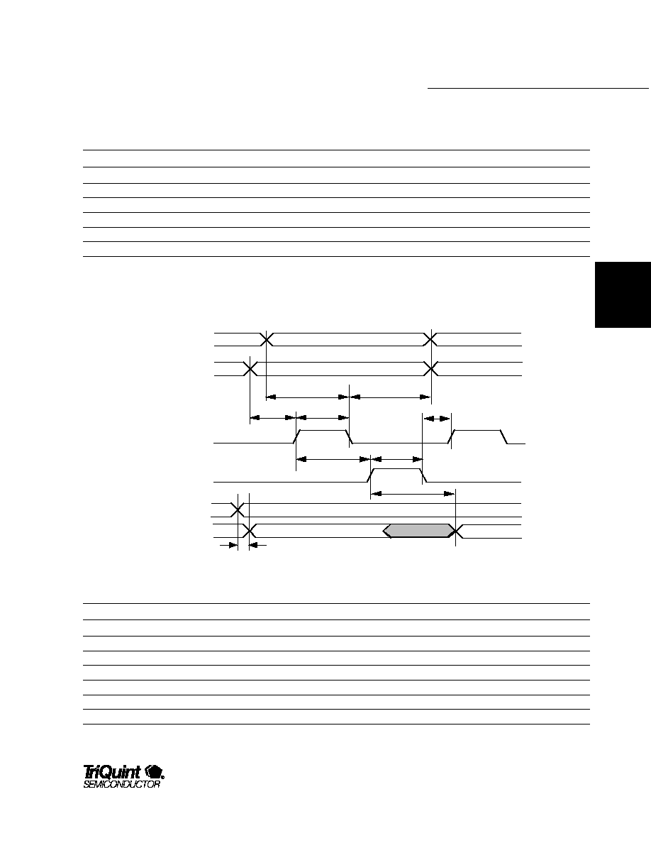
Figure 1. Timing Diagram
Table 6. Timing Specifications
Symbol
Parameter
Minimum
Maximum
Unit
t
sar
Address to Load Set-up time
2
ns
t
har
Address to Load Hold Time
2
ns
t
pwl
Min. Load pulse width
5
ns
t
ldh
Load to Configure delay
0
ns
t
ldl
Configure to Load delay
2
ns
t
pwc
Min. Configure pulse width
5
ns
t
dcf
Configure to Data Valid
20
ns
tsar[OADD]
Tdcf
Tpwl
Tldh
IN
(0:3)
Tpwc
OUT
tsar[IADD]
thar
Data Valid
tldl
Data Not Valid **
** Data remains valid on outputs with unchanged configurations
Input Address
[IADD0:1]
Output Address
[OADD0:1]
CONFIGURE
LOAD
Valid Address
Valid Address
tpd
(0:3)

TQ8004
6
For additional information and latest specifications, see our website: www.triquint.com
Table 7. TQ8004 Pin Descriptions
Signal
Type
Pin Number
Description
Control and Configuration
CONFIGURE
TTL Input
17
Active High. Enables transfer of data from program latches
to configuration latches.
LOAD
TTL Input
16
Active High. Enables program latches to accept new input
address based upon which output is selected using
OADD inputs. Latches address data on de-assertion.
Input Address Control
IADD0
TTL Input
27
Input address LSB
IADD1
TTL Input
28
Input address MSB
Output Address Control
OADD0
TTL Input
14
Output address LSB
OADD1
TTL Input
13
Output address MSB
Output Ports
OUT0,NOUT0
DPECL Output
19,18
True and Complement Differential PECL Data Out
Addressed by OADD(0:1) = 00
OUT1,NOUT1
DPECL Output
21,20
True and Complement DPECL Data Out
Addressed by OADD(0:1) = 01
OUT2,NOUT2
DPECL Output
23,22
True and Complement DPECL Data Out
Addressed by OADD(0:1) = 10
OUT3,NOUT3
DPECL Output
25,24
True and Complement DPECL Data Out
Addressed by OADD(0:1) = 11
Input Ports
IN0,NIN0
DPECL Input
10,11
True and Complement DPECL Data In.
Addressed by IADD(O:1) = 00
IN1,NIN1
DPECL Input
8,9
True and Complement DPECL Data In
Addressed by IADD(O:1) = 01
IN2,NIN2
DPECL Input
6,7
True and Complement DPECL Data In
Addressed by IADD(O:1) = 10
IN3,NIN3
DPECL Input
4,5
True and Complement DPECL Data In
Addressed by IADD(O:1) = 11
Power Pins
Signal
Description
Pin Number
VTT
Input Termination Supply
2
VDD
+3.3V Power Supply
1, 15, 26, Package Down Paddle (required)
GND
Ground Supply
3, 12

TQ8004
7
SWITCHING
PRODUCTS
For additional information and latest specifications, see our website: www.triquint.com
Figure 2. Typical Output Eye with 2
23
-1 PRBS data at 2.7 Gb/s
TQ8004
8
For additional information and latest specifications, see our website: www.triquint.com
Ordering Information
TQ8004
2.7Gbit/sec 4x4 Crosspoint Switch
Additional Information
For latest specifications, additional product information, worldwide sales and distribution locations, and
information about TriQuint:
Web: www.triquint.com
Tel: (503) 615-9000
Email: sales@tqs.com
Fax: (503) 615-8900
For technical questions and additional information on specific applications:
Email: applications@tqs.com
The information provided herein is believed to be reliable; TriQuint assumes no liability for inaccuracies or omissions. TriQuint assumes no
responsibility for the use of this information, and all such information shall be entirely at the user's own risk. Prices and specifications are subject
to change without notice. No patent rights or licenses to any of the circuits described herein are implied or granted to any third party.
TriQuint does not authorize or warrant any TriQuint product for use in life-support devices and/or systems.
Copyright � 2001 TriQuint Semiconductor, Inc. All rights reserved.
Revision 1.0.A
May 2001
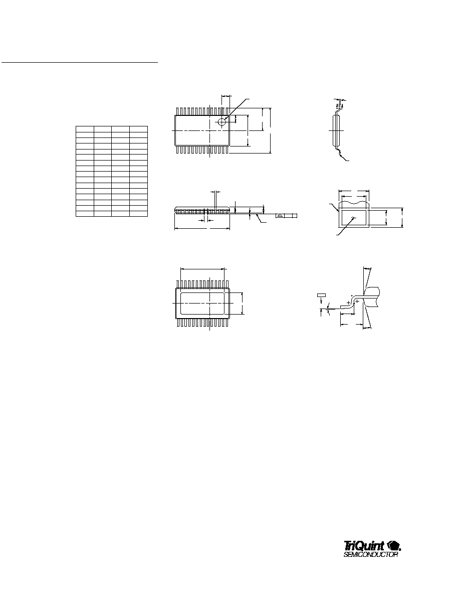
Figure 3. TSSOP Mechanical Dimensions
SIDE VIEW
END VIEW
TOP VIEW
SECTION "B-B"
DETAIL 'A'
B
B
EXPOSED PAD VIEW
MIN
NOM
MAX
A
A1
A2
b
b1
c
c1
D
E1
e
E
L
N
P
P1
1.1262
.0254
.1500
.8500
1.0500
.1900
.3000
.1900
.2500
.0900
.2000
.0900
.1600
9.6000
9.8000
4.3000
4.4000 4.5000
.6500
.6500 .6500
6.4000
.5000
.6000
.7000
28
5.5000
3.0000
3.0100
Note: All dimensions in millimeters (mm).
D
A
e
C
A1
1.00 DIA.
A
2
SEATING
PLANE
1
2
3
SEE
DETAIL "A"
1.00
1.00
aaa
C
L
b1
(b)
(c)
c1
WITH PLATING
BASE METAL
E1
E
E/2
C
b
( )
(VIEW ROTATED 90 C.W.)
0.25
L
P1
P
(14 )
(14 )
(1.00)
C
O
o
o
Moisture Level Rating 3 per
JEDEC Standard J-STD-020A
o
1.10
0.95
5.00