 | –≠–ª–µ–∫—Ç—Ä–æ–Ω–Ω—ã–π –∫–æ–º–ø–æ–Ω–µ–Ω—Ç: TQM7M4014 | –°–∫–∞—á–∞—Ç—å:  PDF PDF  ZIP ZIP |

TQM 7M4014
Description:
Advanced quad-band, compact 3V power amplifier module
designed for mobile handset applications. The small size and
high performance is achieved with high-reliability InGaP HBT
technology. The module is fully integrated, providing a simple
50 Ohms interface on all input and output ports. It includes
internal closed-loop power control. No external matching or
bias components are required. Despite its very compact size,
the module has exceptional efficiency in all bands.
Features:
∑
Very compact size ≠ 10
◊
7
◊
1.4 mm
3
.
∑
High efficiency ≠ typical GSM850 47%,
GSM900 56%, DCS 51%, PCS 50%.
∑
Positive supply voltage ≠ 2.9 to 4.5 V.
∑
50
input and output impedances.
∑
GPRS class 12 compatible.
∑
CMOS band select and internal closed-loop
power control.
∑
High-reliability InGaP technology.
∑
Ruggedness 10:1.
∑
Few external components.
Description:
The module incorporates two highly-integrated InGaP power
amplifier die with a CMOS controller. Each amplifier has three
gain stages with on-die interstage matching implemented with
a high Q passives technology for optimal performance. The
CMOS controller implements a fully integrated closed-loop
power control within the module. This eliminates the need for
any external couplers, power detectors, current sensing etc.,
to assure the output power level. The latter is set directly from
the V
ramp
input from the DAC. The module has Tx enable and
band select inputs. Excellent performance is achieved across
the 824 ≠ 849 MHz, 880 ≠ 915 MHz, 1710 ≠ 1785 MHz, and
1850 ≠ 1910 MHz bands. Module construction is a low-profile
overmolded land-grid array on laminate.
Package Outline:
9.9
9.1
8.4
7.6
6.9
6.1
5.4
4.6
3.9
3.1
2.4
1.6
0.9
0.1
6
.
9
5
.
9
5
.
3
4
.
5
3
.
9
3
.
1
2
.
4
1
.
6
0
.
9
0
.
1
0,0
8.5
1.5
1
.
6
4
.
0
0.9 .05
±
1.32
±
.10
TQS
7M4014
C352
0301
A213505
DCS/PCS-out
V
c
c
2
Band select
12
11
10
9
8
7
6
5
4
3
2
1
20
19
18
17
16
15
14
13
DCS/PCS-in
Tx enable
V batt.
V reg.
V ramp
Cell/GSM in
Cell/GSM out
Vcc
ASIC
V
c
c
2
Dimensions in mm
3V Quad-Band GSM850/GSM900/DCS/PCS Power Amplifier Module
Copyright © 2004 TriQuint Semiconductor Inc., All rights reserved (rev. 20040517)
2
All specifications subject to change without notice
Absolute Maximum Ratings:
Parameter
Symbol
Min.
Max.
Units
Supply voltage
V
bat
-0.3
6.0
V
dc
DC supply current
I
bat
2.4
A
Power control voltage
V
ramp
-0.3
2.2
V
Duty cycle at max. power
50
%
Output load
VSWR
10:1
Operating case temperature
T
c
-25
85
∫C
Storage temperature
T
s
-55
150
∫C
Input power
P
in
11.5
dBm
Note: The amplifier will survive over the full range specified for any individual input, while
other parameters are nominal and with no RF input.
Operating Parameters:
Parameter
Symbol
Min.
Typ.
Max.
Units
Supply voltage
V
bat
2.9
3.5
4.5
V
dc
Supply current Tx
en
High
I
bat
1.8
A
Band select voltage GSM
0
0.5
V
DCS/PCS
2
3.0
Tx enable input Low
0
0.5
High
2
3.0
Regulator voltage
V
reg
2.7
2.8
2.9
V
Regulator current Tx
en
Low
10
Tx
en
High
160
250
Leakage current
Tx
en
Low, Vramp = 0.19V, BS=Low
I
l
1
10
µ
A
Leakage current
Tx
en
Low, Vramp = 0.19V, BS=High
I
l
40
µ
µ
A
V
V
bs
-L
V
bs
-H
Tx
en
I
reg
Moisture Sensitivity Levels:
Required Moisture Sensitivity Level is MSL 3, 240C minimum. Moisture sensitivity classification will
be conducted in accordance with JEDEC J_STD_020B. Table 5.1 of JEDEC J_STD_020B identifies
the floor life for given levels of MSL classification. Floor life is defined as the time from removal of a
device from dry pack until it absorbs sufficient moisture to be at risk during re-flow soldering.
Copyright © 2004 TriQuint Semiconductor Inc., All rights reserved (rev. 20040517)
3
All specifications subject to change without notice
Typical Performance:
GSM850 Electrical Characteristics:
Parameter
Symbol
Min.
Typ.
Max.
Units
Conditions
Frequency Range
f
824
849
MHz
Input Power for P
out
max.
P
in
0.0
2.0
5.0
dBm
33.0
34.5
31.0
32.6
V
bat
= 2.9 V, P
in
= P
in
min.
T
min
T
c
T
max
Power Added Efficiency
40
47
%
P
out
= P
out
max.
Power Control Voltage
V
ramp
0.2
1.6
V
Power Control Current
I
ramp
50
µ
A
Power Control Range
33
36
dB
V
ramp
min
V
ramp
V
ramp
max
Input VSWR
1.5:1
2.5:1
0
P
out
34.5 dBm
Forward Isolation
Iso
-45
-30
dBm
Tx
en
= L, P
in
P
in
max
2f
0
-23
-5.0
3f
0
-20
-10.0
> 3f
0
-10.0
Rx noise power:
869 - 879 MHz
-84
-74.0
dBm
RBW = 100 kHz
879 - 894 MHz
-85
-82.0
P
out
> 5 dBm
Stability
8:1
All phase angles
P
out
34.2 dBm
Ruggedness
10:1
All phase angles
P
out
34.2 dBm
dBm
dBm
Harmonics
Output Power
P
out
Test conditions (unless noted): V
bat
= +3.5 V, V
ramp
= 1.6 V, P
in
= 2 dBm, Duty Cycle =25%, T
c
= 25∫C
Copyright © 2004 TriQuint Semiconductor Inc., All rights reserved (rev. 20040517)
4
All specifications subject to change without notice
GSM900 Electrical Characteristics:
Parameter
Symbol
Min.
Typ.
Max.
Units
Conditions
Frequency Range
f
880
915
MHz
Input Power for P
out
max.
P
in
0.0
2.0
5.0
dBm
34.5
35.0
32.0
33.5
V
bat
= 2.9 V, P
in
= P
in
min.
T
min
T
c
T
max
Power Added Efficiency
50
56
%
P
out
= P
out
max.
Power Control Voltage
V
ramp
0.2
1.6
V
Power Control Current
I
ramp
50
µ
A
Power Control Range
33
36
dB
V
ramp
min
V
ramp
V
ramp
max
Input VSWR
2.5:1
0
P
out
34.5 dBm
Forward Isolation
Iso
-45
-30
dBm
Tx
en
= L, P
in
P
in
max
Cross-band Isolation
Iso
-21
-19
dBm
P
in =
P
in
max., V
bs
= Low
1710
f
1785 MHz
2f
0
-25
-5.0
3f
0
-28
-15.0
> 3f
0
-10.0
Rx noise power:
925 - 935 MHz
-83
-74.0
dBm
RBW = 100 kHz
935 - 960 MHz
-84
-82.0
P
out
> 5 dBm
Stability
8:1
All phase angles
P
out
34.2 dBm
Ruggedness
10:1
All phase angles
P
out
34.2 dBm
dBm
dBm
Harmonics
Output Power
P
out
Test conditions (unless noted): V
bat
= +3.5 V, V
ramp
= 1.6 V, P
in
= 2 dBm, Duty Cycle =25%, T
c
= 25∫C
Copyright © 2004 TriQuint Semiconductor Inc., All rights reserved (rev. 20040517)
5
All specifications subject to change without notice

DCS1800/PCS1900 Electrical Characteristics:
Parameter
Symbol
Min.
Typ.
Max.
Units
Conditions
Frequency Range
f
1710
1850
1785
1910
MHz
Input Power for P
out
max.
P
in
0.0
2.0
5.0
dBm
Output Power
1710 - 1785 MHz
32.0
33.3
29.5
31.2
V
bat
= 2.9 V, P
in
= P
in
min.
T
min
T
c
T
max
1850 - 1910 MHz
31.5
32.5
29.5
30.6
V
bat
= 2.9 V, P
in
= P
in
min.
T
min
T
c
T
max
Power Added Efficiency
%
P
out
= P
out
max.
1710 - 1785 MHz
45
51
T
c
= 25∞C
1850 - 1910 MHz
50
Power Control Voltage
V
ramp
0.2
1.6
V
Power Control Current
I
ramp
50
µ
A
Power Control Range
33
36
dB
V
ramp
min
V
ramp
V
ramp
max
Input VSWR
2.0:1
2.5:1
5
Pout
P
out
max
Forward Isolation
Iso
-38
-30
dBm
Tx
en
= H, P
in
P
in
max
2f
0
-20
-5.0
3f
0
-20
-5.0
> 3f
0
-10.0
Rx noise power
-83.0
-77.0
dBm
RBW = 100 kHz
P
in
= P
in
min., P
out =
P
out
max.
Stability
8:1
All phase angles
P
out
32 dBm
Ruggedness
10:1
All phase angles
P
out
32 dBm
Harmonics
dBm
Test conditions (unless noted): V
bat
= +3.5 V, V
ramp
= 1.6 V, P
in
= 2 dBm, Duty Cycle = 25%, T
c
= 25∫C
P
out
dBm
Copyright © 2004 TriQuint Semiconductor Inc., All rights reserved (rev. 20040517)
6
All specifications subject to change without notice
Pin Out:
Top view
DCS/PCS-out
V
c
c
2
Band select
12
11
10
9
8
7
6
5
4
3
2
1
20
19
18
17
16
15
14
13
DCS/PCS-in
Tx enable
V batt.
V reg.
V ramp
Cell/GSM in
Cell/GSM out
Vcc
ASIC
V
c
c
2
Pin
Symbol
Description
1
RFin - DCS/PCS DCS/PCS power in
2
V
bs
Band select voltage
3
Tx
en
Transmit enable
4
V
bat
Supply voltage
5
V
reg
Regulated voltage input
6
V
ramp
DAC voltage input
7
RF
in
- Cell/GSM GSM850/900 power in
8
V
cc
2
Vcc voltage input
11
RF
out
- Cell/GSM GSM850/900 power out
14
V
cc
V
cc
voltage output
17
RF
out
- DCS/PCS DCS/PCS power out
20
V
cc
2
Vcc voltage input
All other pins are ground
Copyright © 2004 TriQuint Semiconductor Inc., All rights reserved (rev. 20040517)
7
All specifications subject to change without notice
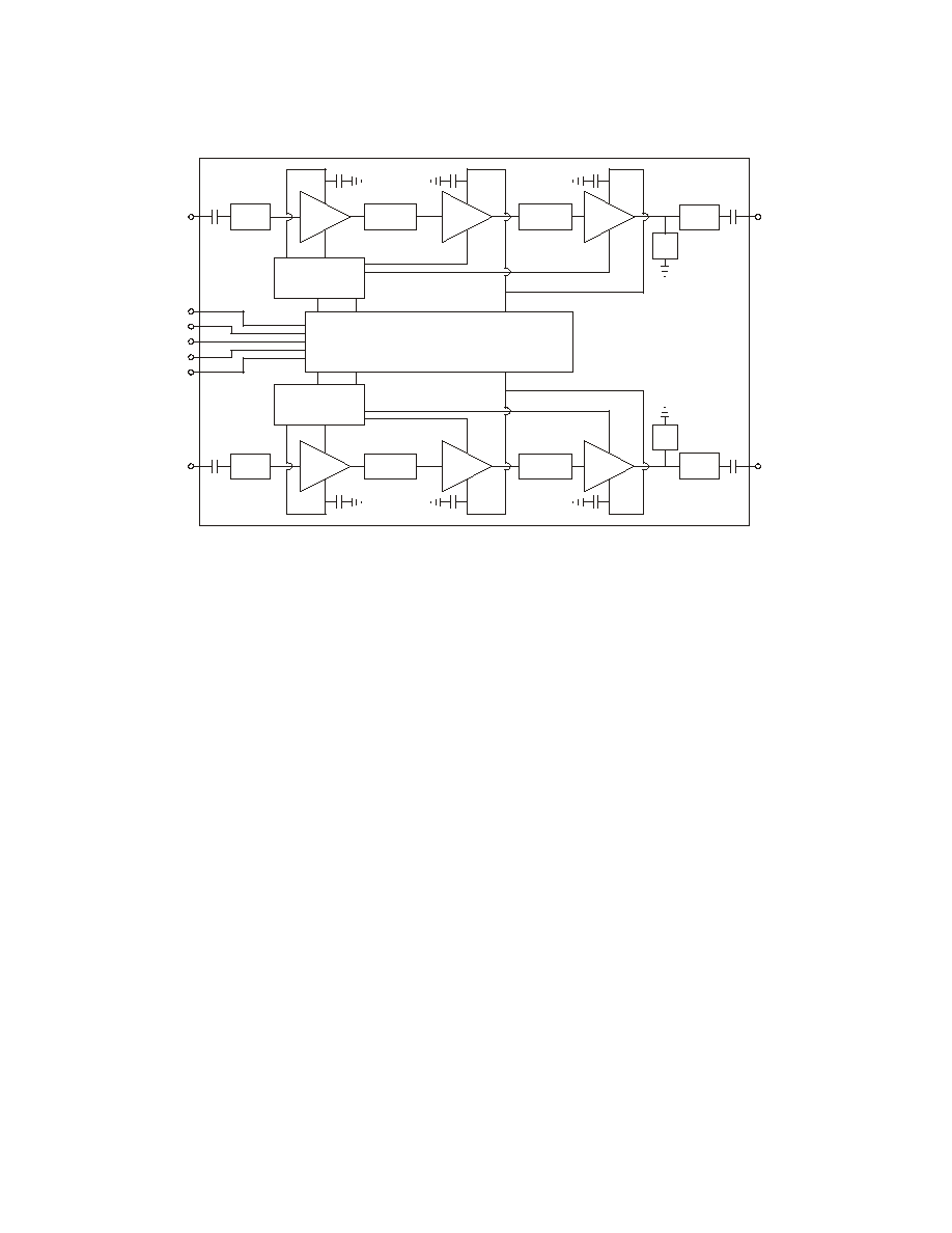
Schematic:
P-out Cell
/GSM
Vramp
Vbat
ASIC
Interstage
Match
ESD
Input
Match
Output
Match
P-in DCS
/PCS
P-out DCS
/PCS
Interstage
Match
Bias
Network
Tx enable
P-in Cell
/GSM
Vreg
Vbs
Input
Match
Interstage
Match
Interstage
Match
Output
Match
ESD
Bias
Network
Copyright © 2004 TriQuint Semiconductor Inc., All rights reserved (rev. 20040517)
8
All specifications subject to change without notice

Tape and Reel Information:
PIN 1
position
Copyright © 2004 TriQuint Semiconductor Inc., All rights reserved (rev. 20040517)
9
All specifications subject to change without notice