 | ÐлекÑÑоннÑй компоненÑ: TS34118 | СкаÑаÑÑ:  PDF PDF  ZIP ZIP |
Äîêóìåíòàöèÿ è îïèñàíèÿ www.docs.chipfind.ru
TS34118
1-20
2004/09 rev. B
TS34118
Voice Switched Speakerphone Circuit
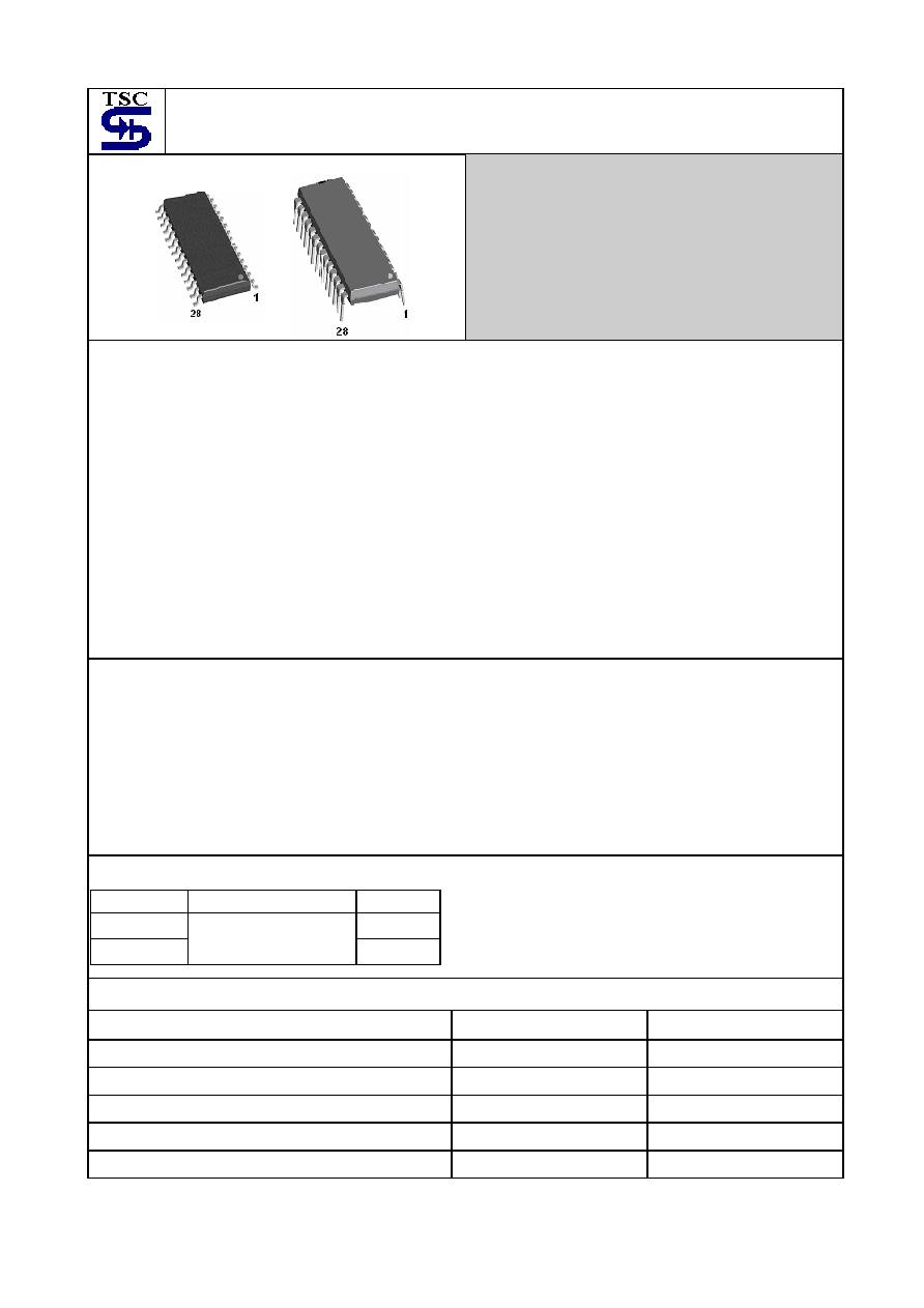
SOP-28 DIP-28
Supply Voltage Range -1.0 V to 7.0V
I
VB
Current 500µA
Microphone Amplifier, & Hybrid Amplifier
Gain 40 dB
General Description
The TS34118 Voice Switched Speakerphone Circuit incorporates the necessary amplifiers, attenuators, level detectors,
and control algorithm to form the heart of a high quality hands-free speakerphone system. Included are a microphone
amplifier with adjustable gain and MUTE control, Transmit and Receive attenuators which operate in a complementary
manner, level detectors at both input and output of both attenuators, and background noise monitors for both the transmit
and receive channels. A Dial Tone Detector prevents the dial being attenuated by the Receive background noise monitor
circuit. Also included are two line drive amplifiers which can be used to form a hybrid network in conjunction with an
external coupling transformer. A high-pass filter can be used to filter out 60Hz noise in the receive channel, or for other
filtering functions .A Chip Disable pin permits powering down the entire circuit to conserve power on long loops where
loop current is at a minimum.
The TS34118 may be operated from a power supply, or it can be powered from the telephone line, requiring typically
5.0mA. The TS34118 can be interfaced directly to Tip and Ring (through a coupling transformer) for stand-alone
operation, or it can be used in conjunction with a handset speech network and/or other features of a feature phone
Features
Improved
attenuator
gain range: 52dB between
transmit and receive.
Low voltage operation for line-powered applications
(3.0-6.5V).
4-point signal sensing for improved sensitivity.
Back ground noise monitors for both transmit
and receive paths.
Standard 28-pin plastic DIP package and SOP
package available.
Microphone amplifier gain set by external
resistors-mute function included.
Chip disable for active/standby operation.
On board filter pinned-out for user defined function.
Dial tone detector to inhibit receive idle mode during
dial tone presence.
Compatible with TS34119 speaker amplifier.
Ordering Information
Part No.
Operating Temp.
Package
TS34118CD DIP-28
TS34118CS
-20 ~ +70
o
C
SOP-28
Absolute Maximum Rating
Description Value
Unit
Supply voltage (pin 4)
-1.0, +7.0
V
Voltage at CD (pin 3), MUT (pin 12)
-1.0,Vcc +1.0
V
Voltage at VLC (pin 13)
-1.0,Vcc +0.5
V
Voltage at TXI (pin 9),RXI (pin 21),FI(pin 2)
-0.5,Vcc +0.5
V
Storage temperature range
-65 to +150
o
C
TS34118
2-20
2004/09 rev. B
Recommended Operating Conditions
Description
Min. Typ. Max. Units
Supply voltage (pin 4) (see Text)
3.5
--
6.5
V
CD input (pin 3), MUT input (pin 12)
0
--
Vcc
V
I
VB
current (pin 15)
-
--
500
µA
VLC (pin 13)
0.3xV
B
-- V
B
V
Attenuator input signal voltage (pin 9,21)
0
--
350
mVrms
Microphone amplifier, Hybrid amplifier gain
0
--
40
dB
Load current @RXO, TXO (pins 8,22)
@MCO (pin 10)
@HTO-, HTO+ (pin 6,5)
0
0
0
--
--
--
±2.0
±1.0
±5.0
mA
Ambient operating temperature range
-20
--
+60
Electrical Characteristics
(T
A
=+25, Vcc=5.0V, CD 0.8V, unless noted)
Parameter
Symbol Min Typ Max Unit
Power Supply
Vcc supply current (Vcc=6.5V, CD=0.8V)
(Vcc=6.5V, CD=2.0V)
Icc
--
--
5.5
600
8.0
800
mA
µA
CD input resistance (Vcc=V
CD
=6.5V)
CD input voltage - High
- Low
R
CD
V
CDH
V
CDL
50
2.0
0
90
--
--
--
Vcc
0.8
K
V
V
V
B
output voltage (Vcc=3.5V)
(Vcc=5.0V)
V
B
--
1.8
1.3
2.1
--
2.4
V
V
B
output resistance (I
VB
=1.0mA) R
OVB
--
400
--
V
B
power supply rejection ratio (C
VB
=220µF,f=1.0KHz)
PSRR -- 54 -- dB
Attenuators
(T
A
=+25)
Receive attenuator gain (f=1.0KHz, V
LC
=V
B
)
Rx model, RXI=150mVrms (Vcc=5.0V)
Rx model, RXI=150mVrms (Vcc=3.5V)
Gain change Vcc=3.5V versus Vcc=5.0V
AGC gain change Vcc=2.8V versus Vcc=5.0V*
Idle model, RXI=150mVrms
Range (Rx to Tx model)
G
RX
G
RX
G
RX1
G
RX2
G
RX1
G
RX3
+4.0
+4.0
-0.5
--
-22
49
+6.0
+6.0
0
-25
-20
52
+8.0
+8.0
+0.5
-15
-17
54
dB
Volume control range (Rx model, 0.3V
B
<V
LC
<V
B
)
V
CR
27
35
--
dB
RXO DC voltage (Rx model)
V
RXO
-- VB -- V
RXO DC voltage (Rx to Tx model)
V
RXO
--
±10
±150
mV
RXO high voltage (Iout=-1.0mA RXI=V
B
+1.5V)
V
RXOH
3.7 -- -- V
RXO low voltage (Iout=+1.0mA, RXI=V
B
-1.0,
Output measured with respect to V
B
)*
V
RXOL
-- -1.5 -1.0 V
RXI input resistance (RXI<350mVrms)
R
RXI
7.0
10
14
K
Transmit attenuator gain (f=1.0KHz)
Tx model , TXI=150mVrms
Idle model, TXI=150mVrms
Range (Tx to Rx model)
G
TX
G
TXI
G
TXI
+4.0
-22
49
+6.0
-20
52
+8.0
-17
54
dB
TXO DC voltage (Tx model)
V
TXO
--
V
B
-- V
TXO DC voltage (Tx to Rx model)
V
TXO
--
±30
±150
mV
TXO High voltage (Iout=-1.0mA TXI=V
B
+1.5V) V
TXOH
3.7 -- -- V
TXO Low voltage (Iout=+1.0mA TXI=V
B
-1.0V,
Output measured with respect to V
B
)*
V
TXOL
-- -1.5 -1.0 V
TS34118
3-20
2004/09 rev. B
Electrical Characteristics
(T
A
=+25, Vcc=5.0V, CD 0.8V, unless noted)
Parameter
Symbol Min Typ Max Unit
Attenuators-continued
(T
A
=+25)
TXI input resistance (TXI<350mVrms)
R
TXI
7.0
10
14
K
Gain tracking (G
RX
+ G
TX
, @ Tx, Idle, Rx)*
G
TR
-- ±0.1 -- dB
Attenuator Control
(T
A
=+25)
C
T
voltage (pin 14-V
B
) Rx model (V
LC
=V
B
)
Idle model
Tx model
V
CT
--
--
--
+240
0
-240
--
--
--
mV
C
T
source current(switching to Rx mode)
I
CTR
-85 -60 -40 µA
C
T
sink current(switching to Tx mode)
I
CTT
+40 +60 +85 µA
C
T
slow idle current
I
CTS
--
0
--
µA
C
T
fast idle internal resistance
R
FI
1.5 2.0 3.6 K
Microphone Amplifier
(T
A
=+25,V
MUT
0.8V,A
VCL
=31dB unless otherwise noted)
Output offset (V
MCO
-V
B
, feedback R=180K) MCOvos
-50
0
+50
mV
Open loop gain (f<100Hz)
A
VOLM
70 80 -- dB
Gain bandwidth
GBW
M
-- 1.0 -- MHz
Output High voltage (Iout=-1.0mA, Vcc=5.0V)
V
MCOH
3.7 -- -- V
Output Low voltage (Iout=+1.0mA)
V
MCOL
-- --
200
mV
Input bias current (@MCI)
I
BM
-- -40 -- nA
Muting (Gain) (f=1.0KHz, V
MUT
=2.0V)
(300Hz<f<10KHz)
GMT
-55
--
--
-68
--
--
dB
MUT input resistance (Vcc=V
MUT
=6.5V) R
MUT
50
90 -- K
MUT Input-High
V
MUTH
2.0 -- Vcc V
MUT Input-Low
V
MUTL
0 --
0.8
V
Hybrid Amplifiers
(T
A
=+25 )
HTO-offset(V
HTO-
-V
B
, Feedback R=51K) H
VOS
-20 0 +20
mV
HTO- to HTO+ offset (Feedback R=51K) HB
VOS
-30 0 +30
mV
Open loop gain(HTI to HTO-, f<100Hz)
A
VOLH
60 80 -- dB
Gain bandwidth
GBW
H
-- 1.0 -- MHz
Closed loop gain(HTO- to HTO+)
A
VCLH
-0.35 0 +0.35
dB
Input bias current(@HTI)
I
BH
-- -30 -- nA
HTO- High voltage (Iout=-5.0mA)
V
HT-H
3.7 -- -- V
HTO- Low voltage (Iout=+5.0mA)
V
HT-L
-- --
250
mV
HTO+ High voltage (Iout=-5.0mA)
V
HT+H
3.7 -- -- V
HTO+ Low voltage (Iout=+5.0mA)
V
HT+L
-- --
450
mV
Distortion(300Hz<f<10KHz, see Figure 1)
THD
H
-- 0.3 -- %
Level Detectors and Background Noise Monitors
(T
A
=+25)
Transmit-Receive switch threshold
(Ratio of current at RLI1 + RLI2 to 20µA
at TLI1 + TLI2 to switch from Tx to Rx)
I
TH
0.8 1.0 1.2
Source current at RLO1, RLO2, TLO1, TLO2
I
LSO
-- -2.0 -- mA
Sink current at RLO1, RLO2, TLO1, TLO2
I
LSK
-- 4.0 -- µA
CPR, CPT output resistance (Iout=1.5mA)
R
CP
-- 35 --
CPR, CPT leakage current
I
CPLK
-- -0.2 -- µA
Filter
(T
A
=+25)
Voltage offset at FO (V
FO
-V
B
, 220K from V
B
to FI)
FO
VOS
-200 -90 0 mV
FO sink current
I
FO
150 260 400 µA
FI bias current
I
FI
-- -50 -- nA
TS34118
4-20
2004/09 rev. B
Electrical Characteristics
(T
A
=+25, Vcc=5.0V, CD 0.8V, unless noted)
Parameter
Symbol Min Typ Max Unit
System Distortion
(T
A
=+25, f=1.0KHz)
Rx mode (from FI to RXO, FO connected to RXI)
THD
R
-- 0.5
3.0
%
Tx mode (from MCI to HTO-/HTO+, includes
Tx attenuator)
THD
T
--
0.8
3.0
%
1. All currents into a device pin are positive, those out of a pin are negative. Algebraic convention rather than magnitude
is used to define limits.
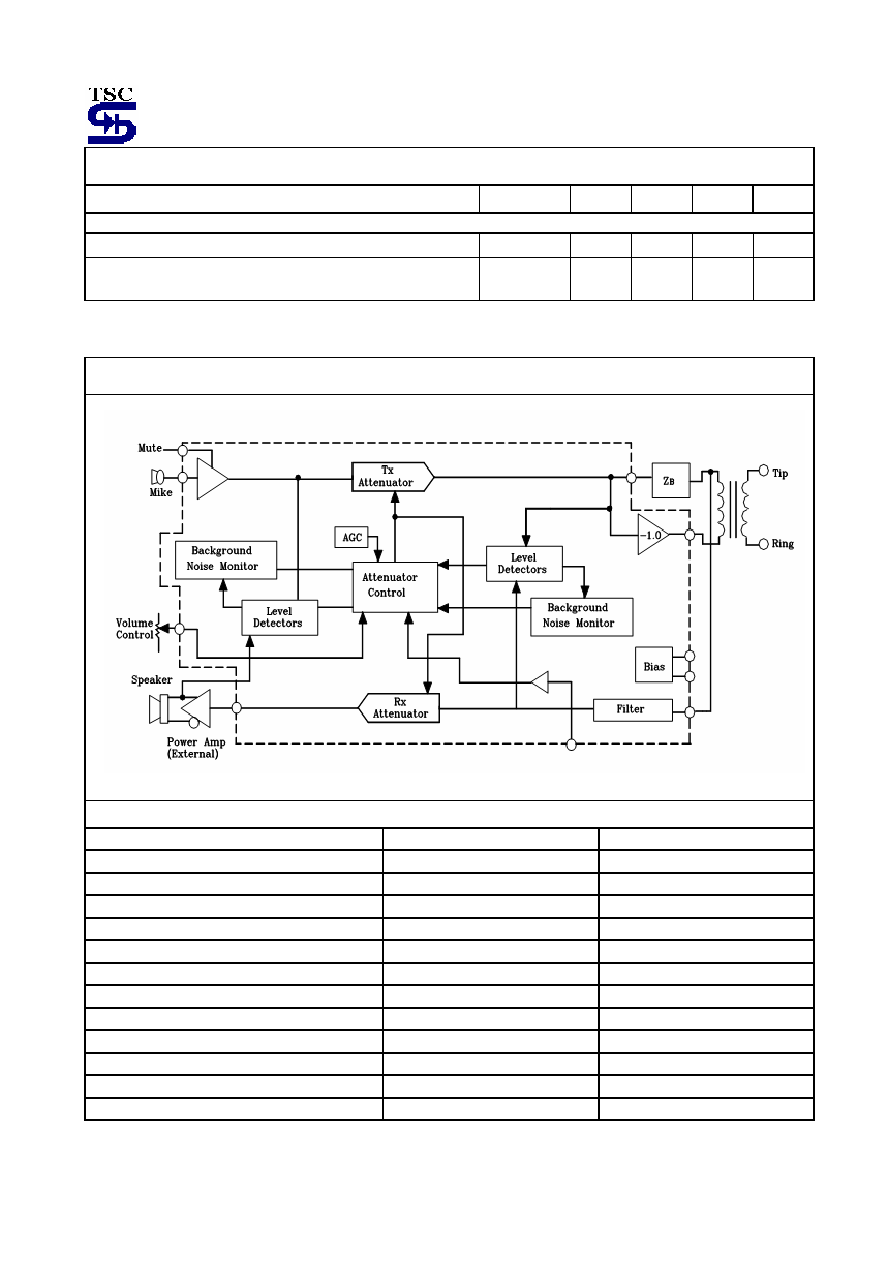
Simplified Block Diagram
Temperature Characteristics
Parameter
Typical Value @25
Typical Change 20 to +60
Vcc supply current (CD=0.8V)
5.0mA
-0.3%/
Vcc supply current (CD=2.0V)
400µA
-0.4%/
V
B
output voltage (Vcc=5.0V)
2.1V
+0.8%/
Attenuator gain (Max Gain) +6.0dB
0.0008dB/
Attenuator gain (Max attenuation) -46dB
0.004dB/
Attenuator input resistance (@ TXI, RXI)
10K +0.6%/
Dial tone detector threshold
15mV
+20µV/
CT source, sink current
±60µA
-0.15%/
Microphone, Hybrid amplifier offset
0 mV
±4.0µV/
Transmit-Receive switching threshold
1.0
±0.02%/
Sink current at RLO1, RLO2, TLO1, TLO2
4.0µA
-10nA/
Closed loop gain (HTO- to HTO+)
0 dB
0.001%/
TS34118
5-20
2004/09 rev. B
Pin Function Description
Pin Name
Description
1
FO
Filter output. Output impedance is less than 50 ohms.
2
FI
Filter input. Input impedance is greater than 1.0Mohm.
3 CD
Chip Disable. A logic low(<0.8V) sets normal operation. A logic high (>2.0V) disables the IC to
conserve power. Input impedance is norminally 90K.
4 Vcc
A supply voltage of +2.8 to +6.5 volts is required, at 5.0mA. As Vcc falls from 3.5 to 2.8volts,
an AGC circuit reduces the receive attenuator gain by 25dB (when in the receive mode).
5 HTO+
Output of the second hybrid amplifier. The gain is internally set at 1.0 to provide a differential
output, in conjunction with HTO-, to the hybrid transformer.
6
HTO-
Output of the first hybrid amplifier. The gain of the amp is set by external resistors.
7
HTI
Input and summing node for the first hybrid amplifier . DC level isV
B.
8
TXO
Output of the transmit attenuator. DC level is approximately V
B.
9
TXI
Input to the transmit attenuator. Max. Signal level is 350m Vrms . Input impedance is 10K.
10
MCO
Output of the microphone amplifier. The gain of the amplifier is set by external resistors.
11
MCI
Input and summing node of the microphone amplifier. DC level is V
B.
12 MUT
Mute input. A logic low(<0.8V) sets normal operation. A logic high (>2.0V) mutes the
microphone amplifier without affecting the rest of the circuit. Input impedance is norminally
90K.
13 VLC
Volume control input. When VLC=V
B
, the receive attenuator is at maximum gain when in the
receive mode. When VLC=0.3V
B
, the receive gain is down 35dB. Does not affect the transmit
mode.
14 C
T
An RC at this pin sets the response time for the circuit to switch modes.
15 V
B
An output voltageVcc/2. This voltage is a system ac ground, and biases the volume control. A
filter cap is required
16
CPT
An RC at this pin sets the time constant for the transmit background monitor.
17
TLI2
Input to the transmit level detector on the mike/speaker side.
18 TLO2
Output of the transmit level detector on the mike/speaker side, and input to the transmit
background monitor.
19
RLO2
Output of the receive level detector on the mike/speaker side.
20
RLI2
Input to the receive level detector on the mike/speaker side.
21 RXI
Input to the receive attenuator and dial tone detector. Max input level is 350mV RMS. Input
impedance is 10K.
22
RXO
Output of the receive attenuator. DC level is approximately V
B
.
23
TLI1
Input to the transmit level detector on the line side.
24
TLO1
Output of the transmit level detector on the line side.
25 RLO1
Output of the receive level detector on the line side, and input to the receive background
monitor.
26
RLI1
Input to the receive level detector on the line side.
27
CPR
An RC at this pin sets the time constant for the receive background monitor.
28
GND
Ground pin for the entire IC.