 | –≠–ª–µ–∫—Ç—Ä–æ–Ω–Ω—ã–π –∫–æ–º–ø–æ–Ω–µ–Ω—Ç: CHX2190A | –°–∫–∞—á–∞—Ç—å:  PDF PDF  ZIP ZIP |

CHX2190a
Ref. : DSCHX21909137
1/4
Specifications subject to change without notice
United Monolithic Semiconductors S.A.S.
Route DÈpartementale 128 - B.P.46 - 91401 Orsay Cedex France
Tel. : +33 (0)1 69 33 03 08 - Fax : +33 (0)1 69 33 03 09
30-60GHz Frequency Multiplier
GaAs Monolithic Microwave IC
Description
The CHX2190a is a cascadable by 2 frequency
multiplier monolithic circuit.
It is designed for a wide range of applications,
from military to commercial communication
systems. The backside of the chip is both RF
and DC grounds. This helps simplify the
assembly process.
The circuit is manufactured with a PM-HEMT
process, 0.15µm gate length, via holes through
the substrate, air bridges and electron beam
gate lithography.
Main Features
Frequency performance : 28-30GHz
4dB conversion loss
DC bias : Vd=3.3V @ Id<3mA
Chip size : 1.47 x 1.12 x 0.10 mm
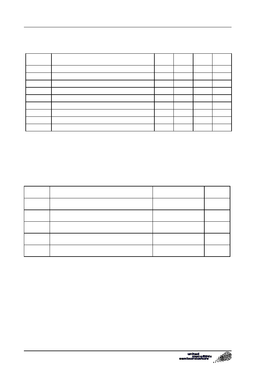
Main Characteristics
Tamb. = 25∞C
Symbol
Parameter
Min
Typ
Max
Unit
Fin
Input frequency range
28
30
GHz
Fout
Output frequency range
56
60
GHz
Pin
Input power
0
3
5
dBm
Lc
Conversion loss
1
4
6
dB
ESD Protection : Electrostatic discharge sensitive device. Observe handling precautions !
CHX2190a
30-60GHz Frequency Multiplier
Ref. : DSCHX21909137
2/4
Specifications subject to change without notice
Route DÈpartementale 128 , B.P.46 - 91401 ORSAY Cedex - FRANCE
Tel.: +33 (0)1 69 33 03 08 - Fax : +33 (0)1 69 33 03 09
Electrical Characteristics
Tamb = +25∞C, Vd = 3.3V
Symbol
Parameter
Min
Typ
Max
Unit
Fin
Input frequency range
28
30
GHz
Fout
Output frequency range
56
60
GHz
Pin
Input power
0
3
5
dBm
Lc
Conversion loss
1
4
6
dB
Harmonic suppression
15
dBc
VSWRin
Input VSWR
2:1
2.3:1
Vd
Drain bias voltage
3.3
3.5
V
Id
Drain current (RF OFF)
3
mA
Vg
Gate voltage
-1.4
-1
-0.7
V
(1) With an Off chip 180∞ IF Divider
Absolute Maximum Ratings
(1)
Tamb = +25∞C
Symbol
Parameter
Values
Unit
Vd
Drain bias voltage
4
V
Vg
Gate bias voltage
-2
V
Pin
Maximum peak input power overdrive (2)
+15
dBm
Top
Operating temperature range
-40 to +85
∞C
Tstg
Storage temperature range
-55 to +125
∞C
(1) Operation of this device above anyone of these paramaters may cause permanent damage.
(2) Duration < 1s.
30GHz Frequency Multiplier
CHX2190a
Ref. : DSCHX21909137
3/4
Specifications subject to change without notice
Route DÈpartementale 128 , B.P.46 - 91401 ORSAY Cedex - FRANCE
Tel.: +33 (0)1 69 33 03 08 - Fax : +33 (0)1 69 33 03 09
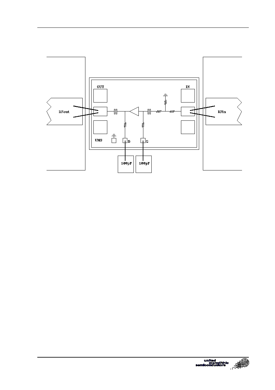
Chip Assembly and Mechanical Data
Note : Supply feed should be capacitively bypassed. 25
µ
m diameter gold wire is to be prefered.
CHX2190a
30-60GHz Frequency Multiplier
Ref. : DSCHX21909137
4/4
Specifications subject to change without notice
Route DÈpartementale 128 , B.P.46 - 91401 ORSAY Cedex - FRANCE
Tel.: +33 (0)1 69 33 03 08 - Fax : +33 (0)1 69 33 03 09
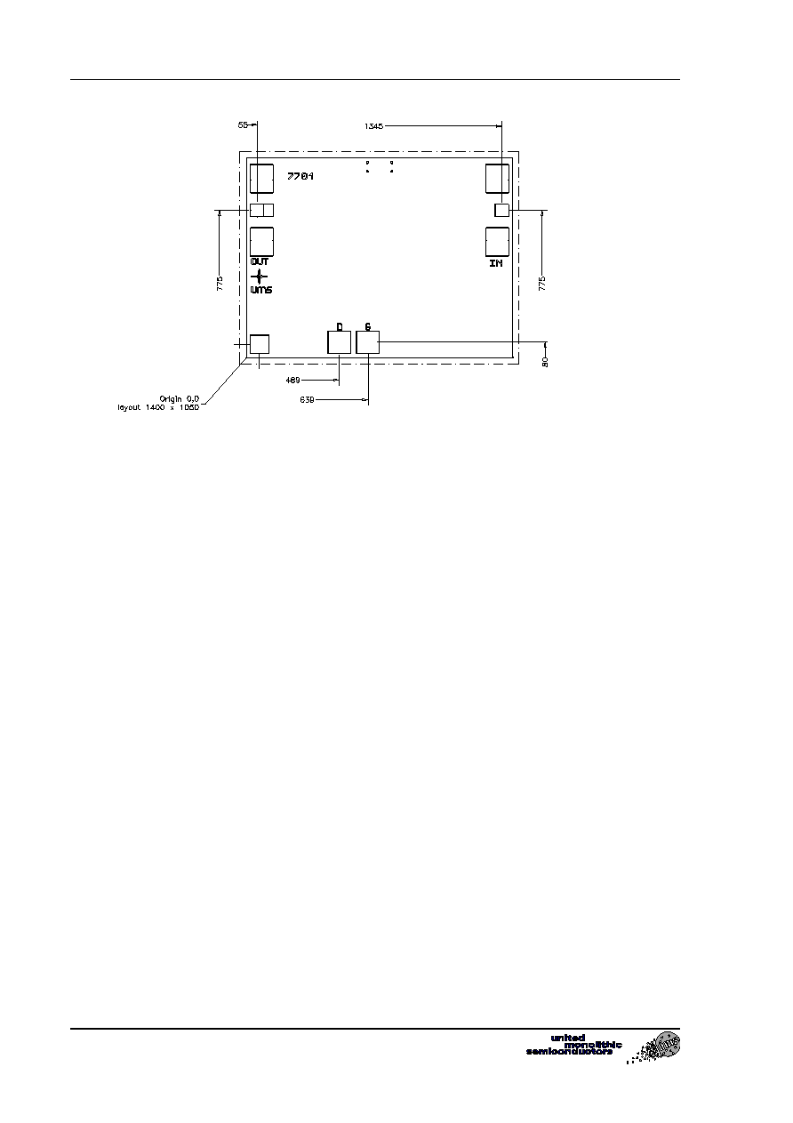
Bonding pad positions.
( Chip thickness : 100µm. All dimensions are in micrometers )
Information furnished is believed to be accurate and reliable. However United Monolithic Semiconductors
S.A.S. assumes no responsability for the consequences of use of such information nor for any infringement of
patents or other rights of third parties which may result from its use. No license is granted by implication or
otherwise under any patent or patent rights of United Monolithic Semiconductors S.A.S.. Specifications
mentioned in this publication are subject to change without notice. This publication supersedes and replaces all
information previously supplied. United Monolithic Semiconductors S.A.S. products are not authorised for
use as critical components in life support devices or systems without express written approval from United
Monolithic Semiconductors S.A.S.