
VIA Technologies, Inc.
Preliminary VT86C100A
VT86C100A
PCI F
AST
E
THERNET
C
ONTROLLER
DATA SHEET
(Preliminary)
DATE : Aug 31, 1997
VIA TECHNOLOGIES, INC.

VIA Technologies, Inc.
Preliminary VT86C100A
P
RELIMINARY
R
ELEASE
Please contact Via Technologies for the latest documentation.
Copyright Notice:
Copyright
�
1995, Via Technologies Incorporated. Printed in Taiwan. A
LL
R
IGHTS
R
ESERVED
.
No part of this document may be reproduced, transmitted, transcribed, stored in a retrieval system,
or translated into any language, in any form or by any means, electronic, mechanical, magnetic,
optical, chemical, manual or otherwise without the prior written permission of Via Technologies
Incorporated.
The VT86C100A may only be used to identify products of Via Technologies.
All trademarks are the properties of their respective owners.
Disclaimer Notice:
No license is granted, implied or otherwise, under any patent or patent rights of Via Technologies.
Via Technologies makes no warranties, implied or otherwise, in regard to this document and to the
products described in this document. The information provided by this document is believed to be
accurate and reliable to the publication date of this document. However, Via Technologies
assumes no responsibility for any errors in this document. Furthermore, Via Technologies assumes
no responsibility for the use or misuse of the information in this document and for any patent
infringements that may arise from the use of this document. The information and product
specifications within this document are subject to change at any time, without notice and without
obligation to notify any person of such change.
Offices:
5020 Brandin Court
8th Floor, No. 533
Fremont, CA
94538
Chung-Cheng Rd., Hsin-Tien
USA
Taipei, Taiwan ROC
Tel:
(510) 683-3300
Tel:
(886-2) 218-5452
Fax:
(510) 683-3301
Fax:
(886-2) 218-5453
Onlines Services:
BBS : 886-2-2186408
FTP : FTP.VIA.COM.TW
HTTP: WWW.VIA.COM.TW

VIA Technologies, Inc.
Preliminary VT86C100A
VT86C100A PCI F
AST
E
THERNET
C
ONTROLLER
F
EATURES
* Single chip Fast Ethernet controller for PCI bus interface
--
compliant to PCI v2.1 with optional delay transaction and sub-vendor, sub-system- ID
--
Provides a direct connection to PCI bus
--
Supports two network ports : 10/100 M MII interface
* High performance PCI mastering structure
-- VIA self-define 128 bytes memory I/O or register I/O based command and status register
--
Software oriented chain structure description to minimize hardware complexity
-- Include on chip bus master DMA with programmable burst length for low CPU utilization
-- Dynamic transmit packet auto queuing for back auto queuing for bac for back to back transmissin
-- Programmable activity polling intervals for description DMA
-- Programmable DMA arbitration priority to minimize overflow under flow condition
-- Support early receive and early transmit interrupt for software parallel processing
-- Interrupt controllable by receive/transmit descriptor list for saving interrupt service time
* Provides standard 100-M bits MII interface
--
Support 100Base-TX with CAT5 UTP, STP and fiber cables
-- Support 100Base-T4 with CAT3, CAT4, CAT 5 UTP, STP
* 10/100Mhz full duplex, half duplex operation
* Contains two deeper 2K bytes FIFO for receive and transmit controller both supports bursts of
up to full Ethernet length
--
Programmable receive and transmit FIFO threshold control for optimize PCI throughput
* Flexible dynamically load EEPROM algorithm.
--
Load after power-up
--
Dynamic auto reload
--
Embedded programming for configure modification
--
Dynamic direct programming for manufacturing
* Support physical, Broadcast, Multicast address filtering using hashing function
* Support Magic packet and wake on address filtering
* Support external Bootrom up to 64K bytes no external address latch
* Software controllable power down feature
* Single +5V supply, 0.5um standard CMOS technology
* 128 pin PQFP package
VIA Technologies, Inc.
Preliminary VT86C100A
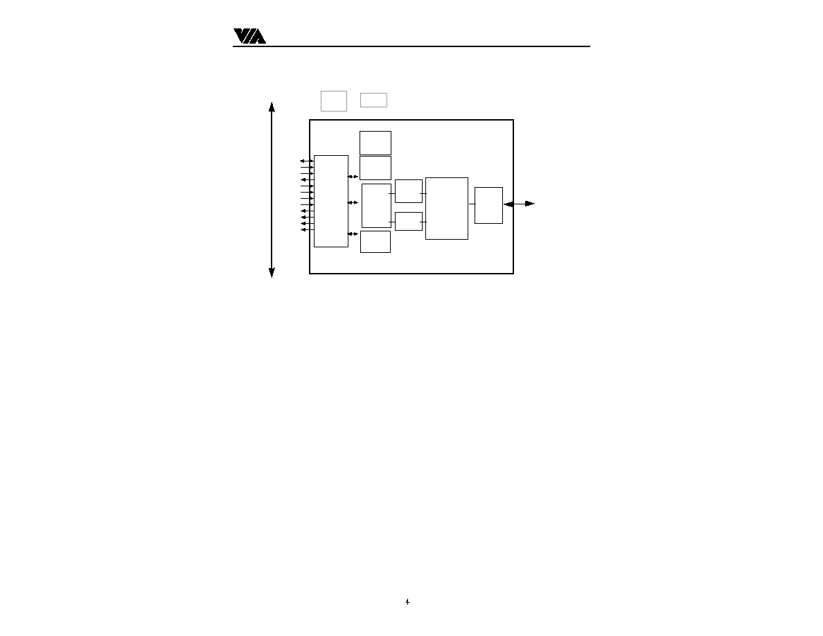
Configuration
Registers &
EEPROM Control
10/100M
MAC Tx/Rx
Protocol
State
Tally Counters
Boot
ROM
Config.
EEPROM
Master
Registers
&
State
Machine
&
Buffer
Mgmt.
PCI CFG
MII
_MSRD,
_MSWR,
EECS
PCI
Bus
AD[31:0]
PCICLK
PCIRST#
INTA#
CBE#[3:0]
IDSEL
FRAME#
IRDY#
TRDY#
DEVSEL#
STOP#
PAR
Interface
Unit
RxFIFO
TxFIFO
2K bytes
2K bytes
TXD[3:0],
RXD[3:0],
TX_EN
TX_CLK, RX_CLK
TX_ER, RX_ER
RX_DV, CRS, COL
MDIO
PCI v2.1
Figure 1: Application Diagram
VIA Technologies, Inc.
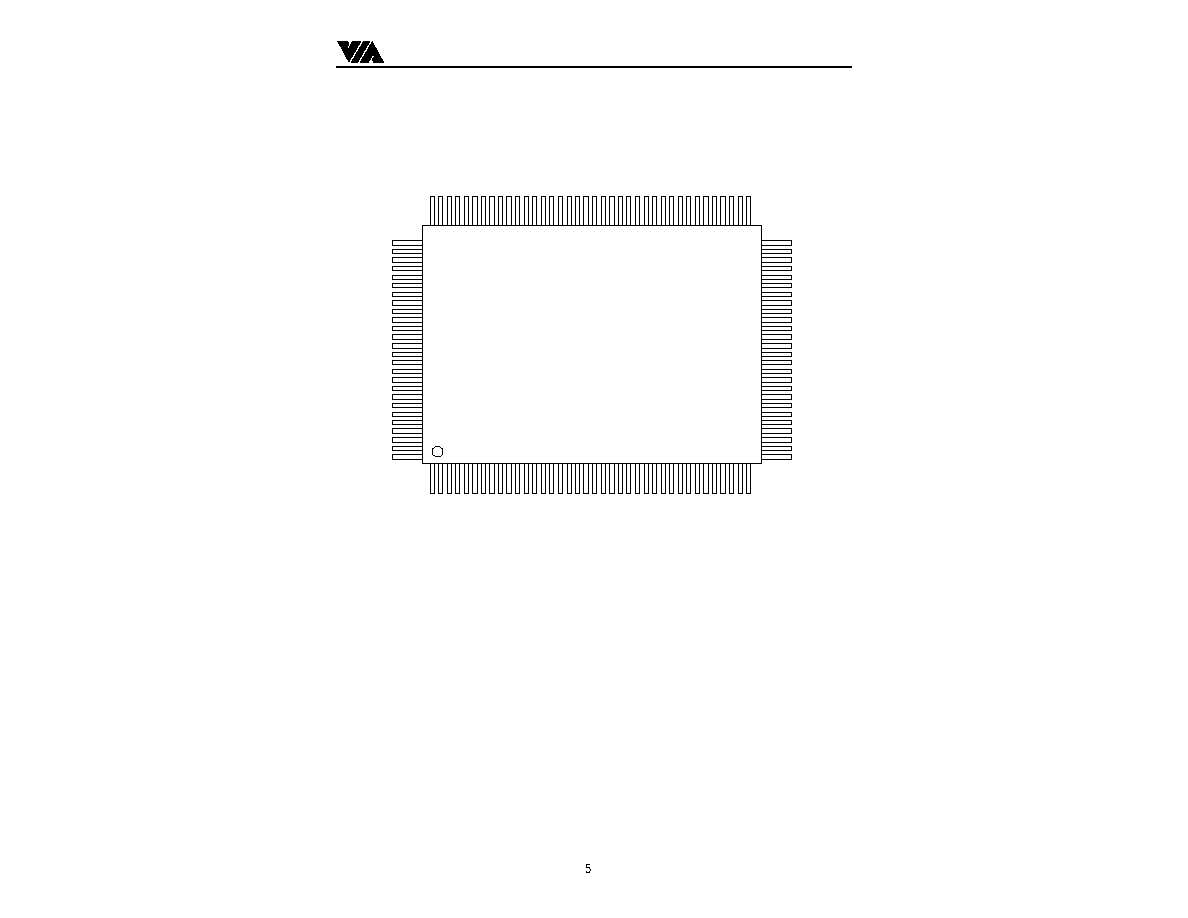
Preliminary VT86C100A
P
IN
D
IAGRAM
VT86C100A
1
39
3
8
3
5
3
0
2
5
2
0
1
5
1
0
5
1
0
2
1
0
0
6
5
7
0
7
5
8
0
8
5
9
0
9
5
64
60
55
50
45
128
103
105
110
115
120
125
AD25
AD24
CEB3#
IDSEL
AD23
VSS
AD22
AD21
AD20
AD19
AD18
AD17
VDD
AD16
VSS
CBE2#
FRAME#
IRDY#
TRDY#
DEVSEL#
STOP#
VDD
PERR#
VSS
PAR
CBE1#
AD15
AD14
AD13
AD12
AD11
AD10
VSS
VDD
AD9
AD8
CBE0#
AD7
AD6
AD5
AD3
VSS
AD2
AD1
VDD
AD4
AD0
ECS
BPRD#
MD0
VSS
MD1
MD2
MD3
MD4
MD5
MD6
VDD
MD7
VSS
NC
NC
RAMVDD
RAMVSS
MA0
MA1
MA2
MA3
MA4
MA5
MA6
VSS
VDD
MA7
MA8
MA9
MA10
MA11
MA12
MA13
MA14
VSS
MA15
GPIO1/AUXPME
VDD
NC2
VDD
VSS
MDC
MRXD0
MRXD1
MRXD2
MRXD3
VDD
VSS
MDIO
HDRST
M10TEN
INTA#
PCIRST#
PCICLK
VSS
VDD
PME#
GNT#
REQ#
AD31
AD30
AD29
AD28
VDD
VSS
AD27
AD26
TST
MCRS
MCOL
MTXD3
MTXD2
MTXD1
MTXD0
MTXE
VDD
VSS
MTXC
MERR
MRXC
MRXDV

VIA Technologies, Inc.
Preliminary VT86C100A
P
IN
D
ESCRIPTIONS
No.
Name
Type
Description
PCI Bus Interface
121-
124,127-
128,1-
2,5,7-
9,11-
14,27-
32,35-
36,38,39-
40,42-46
AD31-0
I/O
Address/Data are multiplexed on the same PCI pins. A bus transaction
consists of an address phase followed by one or more data phases. The
address phase is the clock cycle in which FRAME# is asserted. Write
data is stable and valid when IRDYB is asserted and read data is stable
and valid when TRDYB is asserted.
115
PCICLK
I
PCICLK provides timing for all transactions on PCI and is an input pin
to every PCI device.
113
INTA#
OD
INTA# is an asynchronous signal which is used to request an interrupt
114
PCIRST#
I
When PCIRST# is asserted low, the VT86C100A chip performs an
internal system hardware reset. PCIRST# may be asynchronous to CLK
when asserted or deasserted. It is recommended that the deassertion be
synchronous to guarantee clean and bounce free edge.
3,16,26,37
CBE#[3:0]
I
Bus Command/Byte Enables are multiplexed on the same PCI pins.
During the address phase of a transaction, CBE3-0B define the Bus
Command. Burring the data phase, CBE3-0B are used as Byte Enables.
The Byte Enables define which physical byte lanes carry meaningful
data. CBE0B applies to byte 0 and CBE3B applies to byte 3.
4
IDSEL
I
Used as a chip select during PCI configuration cycle.
17
FRAME#
I/O
Cycle Frame is driven by the current master to indicate the beginning
and duration of an access. FRAME# is asserted to indicate a bus
transaction is beginning. While FRAME# is asserted, data transfers
continue. When FRAME# is deasserted, the transaction is in the final
data phase.
18
IRDY#
I/O
Initiator Ready indicates the initiating agent's ability to complete the
current data phase of the transaction. IRDY# is used in conjunction with
TRDY#. A data phase is completed on any clock when both IRDY# and
TRDY# are asserted. During a write, IRDY# indicates that valid data is
present on AD31-0. During a read, it indicates the master is prepared to
accept data. Wait cycles are inserted until both IRDY# and TRDY# are
asserted simultaneously.
19
TRDY#
I/O
Target Ready indicates the target's agent's ability to complete the current
data phase of the transaction. TRDY# is used in conjunction with
IRDY#. A data phase is completed on any clock when both IRDY# and
TRDY# are asserted. During a read, TRDY# indicates that valid data is
present on AD31-0. During a write, it indicates the target is prepared to
accept data. Wait cycles are inserted until both IRDY# and TRDY# are
asserted simultaneously.
20
DEVSEL#
I/O
Device Select, when actively driven, indicates the driving device has
decoded its address as the target of the current access. As an input,
DEVSEL# indicates whether any device on the bus has been selected.
21
STOP#
I/O
VT86C100A drives STOP# to disconnect further traction.

VIA Technologies, Inc.
Preliminary VT86C100A
25
PAR
T/S
Parity is even parity across AD31-0 and CBE3-0B. PAR is stable and
valid one clock after the address phase. For data phases PAR is stable
and valid one clock after either IRDY# is asserted on a write transaction
or TRDY# is asserted on a read transaction.
118
GNT#
I
Bus grant asserts to indicate to the VT86C100A that access to the bus is
granted.
119
REQ#
O
Bus request is asserted by the bus master indicate to the bus arbiter that
it wants to use the bus.
23
PERR#
I/O
Parity error asserts when a data parity error is detected
120
PME#
O
Power management event interrupt
111
HDRST
O
When PCIRST# is asserted low, the VT86C100A chip performs an
internal system hardware reset. Then HDRST is asserted high for
external device reset signal like PHY device.
Network Interface
91
MCOL
I
Collision detect when the external PHY device
90
MCRS
I
Carrier sense is asserted by the external PHY when the media is active
92-95
MTXD[3-0]
O
MII 4 parallel transmit data lines. This data be synchronized to assertion
by the MTXC signal
96
MTXEN
O
Transmit enable signals that the transmit is active in the MII port to an
external PHY device
99
MTXC
I
MII transmit clock supports the 25mhz or 2.5mhz transmit clock
supplied by the external PMD device. This clock should always be
active.
100
MERR
I
MII receive error asserts when a data decoding error is detected by
external PHY device.
101
MRXC
I
MII receive clock supports the 25mhz or 2.5mhz clock. This clock is
recovered by the PHY.
102
MRXDV
I
MII data valid
103-106
MRXD[0-3]
I
Four parallel receive data lines. This data be driven from external PHY
be synchronized with MRXC signal.
109
MDC
O
MII management data clock be soured by VT86C100A MDC bit
(MIIR:0) to the external PHY devices as timing reference for the
MDIO signal.
110
MDIO
I/O
MII management data input/output, read from MDI bit (MIIR:1) or
written from MDO bit (MIIR:2)
112
GPIO
I/O
GPIO
External Memory Support & General purpose I/O support
49
EECS
O
EEPROM Chip Select: Chip select signal for the external EEPROM
when a EEPROM is used to provide the configuration data and
Ethernet Address. A 100K pull-up resistor is connected.
50
BPRD#
O
Boot PROM Read: Read the Boot ROM on the memory support data
bus.
51
MD0/
EEDO
I/O
Bootrom data 0
Serial ROM Data output
52
MD1/
EEDI
O/O
Bootrom data 1
Serial ROM Data input
53
MD2/ EECLK
O/O
Bootrom data 2
Serial ROM Clock signal
54-55,58-
60
MD3-7
I/O
Bootrom Data [3-7] :

VIA Technologies, Inc.
Preliminary VT86C100A
63-64,67-
73,78-
84
MA0-MA15
O
Bootrom address line [0-15]
85
GPIO1/AUXP
ME
IO
General purpose input and output 1 : usually as Magic key interrupt line
112
GPIO2/LKC
IO
General purpose input and output 2, this pin usually as link change status
from external PHY device.
Power Supply & Ground
10,22,34,47,
56,65,76,
87,97,108
,117,125
VDD, VDDA
P
Positive 5V Supply: Supply power to Internal digital logic, Digital I/O
pads, and TD, TX pads. Double bonding may be required.
6,15,24,33,
41,48,57
,66,75,7
7,88,98,
107,116,
126
VSS, VSSA
G
Negative Supply: digital ground. Multiple bonding pads are
required to separate core and I/O pads ground.

VIA Technologies, Inc.
Preliminary VT86C100A
F
UNCTIONAL
D
ESCRIPTIONS
1. G
ENERAL
D
ESCRIPTION
The VT86C100A Rhine ACPI PCI bus master 100 M FAST Ethernet controller is CMOS VLSI designed for
easy implementation of CSMA/CD IEEE 802.3u 100M local area networks. Significant features include:
twisted-pair interface, PCI Plug&Play compatibility, 32 bit bus mastering, powerful buffer management and
Early Interrupt Receive/Transmit.
The VT86C100A integrates the entire bus interface of PCI systems. Setting hardware jumpers or software
configures the VT86C100A bus interface. The VT86C100A also complies with PCI specification v2.1.. The
VT86C100A supports the Media Independent Interface (MII) network interface.
1.1 FIFO A
ND
C
ONTROL
L
OGIC
The VT86C100A incorporates two independent 2K bytes deeper FIFO for transmit or receive data from
system interface or to the network interface, providing temporary storage of data, free host system from the
real-time demands on network.
The VT86C100A enhanced the FIFO management logic to handle received data packets up to four packets
before transfer to system data buffer. This ability reduce the packets losing due to PCI bus mastering abrition
latency.
2. N
ETWORK
I
NTERFACE
The VT86C100A Rhine ACPI support one MII interface
2.1 MII Interface
The MII interface is an IEEE 802.3 compliant interface that provides a simple and easy interconnection
between the MAC layer and PHY device. This interface has support the following characteristics :
�
Support both 10M and 100M data rate.
�
Contains data and synchronous clock
�
4-bit independent receive and transmit data.
�
Uses TTL signal levels and compatibles with common CMOS processes.

VIA Technologies, Inc.
Preliminary VT86C100A
3.
EEPROM Interface and Programming
VT86C100A uses an 93C46 to store configuration data and Ethernet address.
3
.1. EEPROM Contents
D15
D0
3FH
.
.
.
Reserved for 93C46
.
.
.
Reserved for 93C46
.
.
.
.
.
.
10H
.
.
.
.
.
.
.
.
0FH
73H
73H
0EH
CFG_D
CFG_C
0DH
CFG_B
CFG_A
0CH
BCR1
BCR0
0BH
MAX_LAT
MIN_GNT
0AH
Reserved
Reserved
09H
KEY5
KEY5
08H
KEY3
KEY2
07H
KEY1
KEY0
06H
Reserved
Reserved
05H
SUBVID1
SUBVID0
04H
SUBSID1
SUBSID0
03H
Reserved
Reserved
02H
Ethernet Address 5
Ethernet Address 4
01H
Ethernet Address 3
Ethernet Address 2
00H
Ethernet Address 1
Ethernet Address 0
Note 1. The word on location 03H is optional to user's application requirement.
Note 2. Programming 73H into the upper address is required to protect the Ethernet address from being destroyed accidentally
Note 3. The word on location 04H, 05H is sub-System ID, sub-Vendor ID in PCI specification 2.1.
3.2. D
IRECT
P
ROGRAMMING OF
EEPROM
The VT86C100A features a easy way to program external EEPROM in-situ. When the RESET is active and if
the upper byte of 0FH on EEPROM is not 73H, the EEPR bit will not be set to indicate that the current
EEPROM has not been programmed yet. This will allow the VT86C100A to enter Direct Programming mode
if EELOAD is also set. In this mode the user can directly control the EEPROM interface signals by writing to
the ECSR Port and the value on the EECS, ESK and EDI bits will be driven onto the EECS, SK(MD2), and
DI(MD1) outputs respectively. These outputs will be latched so the user can generate a clock on SK by
repetitively writing 1 then 0 to the appropriate bit. This can be used to generate the EEPROM signals as per
the 93C46 data sheet.
To read the EEPROM data, users have to generate EEPROM interface signals into EECS, DI and SK as
described above and in the mean time read the data from DO(MD0) input via pin SD0. Reading Data
Transfer Port during programming will not affect the latched data on EECS, SK, and DI outputs. When the

VIA Technologies, Inc.
Preliminary VT86C100A
EEPROM has been programmed and verified (remember to program the upper byte of 0EH & 0FH with
73H), the user must give VT86C100A a power-on reset to return to normal operation and to read in the new
data.
The Direct Programming mode is mainly used for production to program every bit of the EEPROM. Once the
upper byte of 0EH has been programmed with 073H and a power-on reset has been performed, there is no
way to change the contents of EEPROM except Configuration Registers A, B, and C, which will be discussed
in the following paragraph. For more information, refer to EECSR.
3.3. E
MBEDDED
P
ROGRAMMING OF
EEPROM
If the upper byte of 0FH of EEPROM has been programmed to 073H when VT86C100A is loading the
EEPROM data during power-on reset, the EEPR bit of Signature Register will be set to prohibit the Direct
Programming mode. However, the user can still program the configuration registers A, B, and C using the
Embedded Programming mode by following the routine specified in the pseudo code below. This operation
will work regardless of the value of EECONFIG. The setting of the EELOAD bit of Configuration Register B
starts the EEPROM write process. Care should be taken not to accidentally modify the POL and GDLNK bits
because these two bits return the value indifferent from the setting. This programming process is ended when
the EELOAD bit goes to zero.
EEPROM_EMB_PROG ( )
// defined constant:
CONFIG_B, EELOAD
// declared register: value, config_for_A, config_for_B, config_for_C
// declared function: DISABLE_INTERRUPTS, ENABLE_INTERRUPTS, READ, WRITE, WAIT
DISABLE_INTERRUPTS ( );
value = READ (
CONFIG_B);
value = value |
EELOAD;
WRITE (
CONFIG_B, value);
READ (
CONFIG_B);
WRITE (
CONFIG_B, config_for_A);
WRITE (
CONFIG_B, config_for_B);
WRITE (
CONFIG_B, config_for_C);
while (value ||
EELOAD)
{
value = READ (
CONFIG_B);
WAIT ( );
}
ENABLE_INTERRUPTS ( );
VIA Technologies, Inc.
Preliminary VT86C100A
4. PCI Configuration Space
Device ID
( 6100 )
Vendor ID
( 1106 )
00 h
STATUS
(DEVS1, DEVS0 ) = ( 1 , 0 )
COMMAND
( MMSPACE, IOSPACE)
04 h
CLASS CODE
( 02_00_00 )
Revision ID
( 04 )
08 h
BIST
( 00 )
Header type
( 00 )
Latency Timer
( R/W )
Cache Line
( R/W )
0c h
CSR Memory Map Base Addr 000
0
0 0 1
10 h
CSR IO MAP SPACE 000
0
0 0 0
14 h
Sub-System ID
Sub-Vendor ID
2c h
EXP ROM BASE [ 31: 15 ]
ROM14
0000_0000_00000
EN
30 h
Reserved
Reserved
Max_LAT
( 00 )
Min_GNT
( 00 )
INT PIN
( 01 )
INTLINE
INTL [7:0]
3c h
Reserved
Reserved
MODE3
MODE2
FIFOTST
MODE0
50H
5. M
AGIC
K
EY
F
ILTERING AND
W
AKE ON
M
AGIC
K
EY
The VT86C100A provides an one level power down mode. The BIOS or Network OS device driver can
configure Register A to diagnostic mode then set the Power-on bit of the diagnostic port to "on." When the
VT86C100A is in Power down mode, all power to the PCI interface is cut off and the chip clock is stopped.
Other registers are read only. Only the diagnostic port is read/writeable.
The VT86C100A can store one "Magic Key" (6 bytes Ethernet address) as external trigger event. When
VT86C100A received one Magic Key address packet, the PME# or GPIO1 will be generated to system.
These signal can be asserted to ATX power PS-ON (refere to ATX specification v2.01) or mother board wake
up interrupt line like ring-in.
VIA Technologies, Inc.
Preliminary VT86C100A
6. B
UFFER
M
ANAGEMENT
& H
OST
C
OMMUNICATION
The VT86C100A provides an simply and effective buffer management and host communication
method through the PCI Bus mastering : There are two descriptor lists, one for receive and one for transmit.
The base of these two list are pointed into the CRDA (18h) and CTDA (1ch) registers.
The descriptor list reside in the host physical memory address space with double word boundary.
And each descriptor lists just point to one single buffer, but a data buffer consists of either an entire frame or
part of a frame. Data chain can be enabled or disabled by DES1 C bit. Data buffer also reside in host physical
memory double word boundary space.
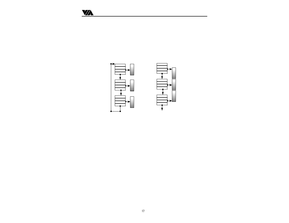
The device driver can make the last descriptors next link be point to first descriptor address, become
a ring buffer structure.
Descriptor 0
Buffer 1
Descriptor 1
Buffer 1
Next Descriptor
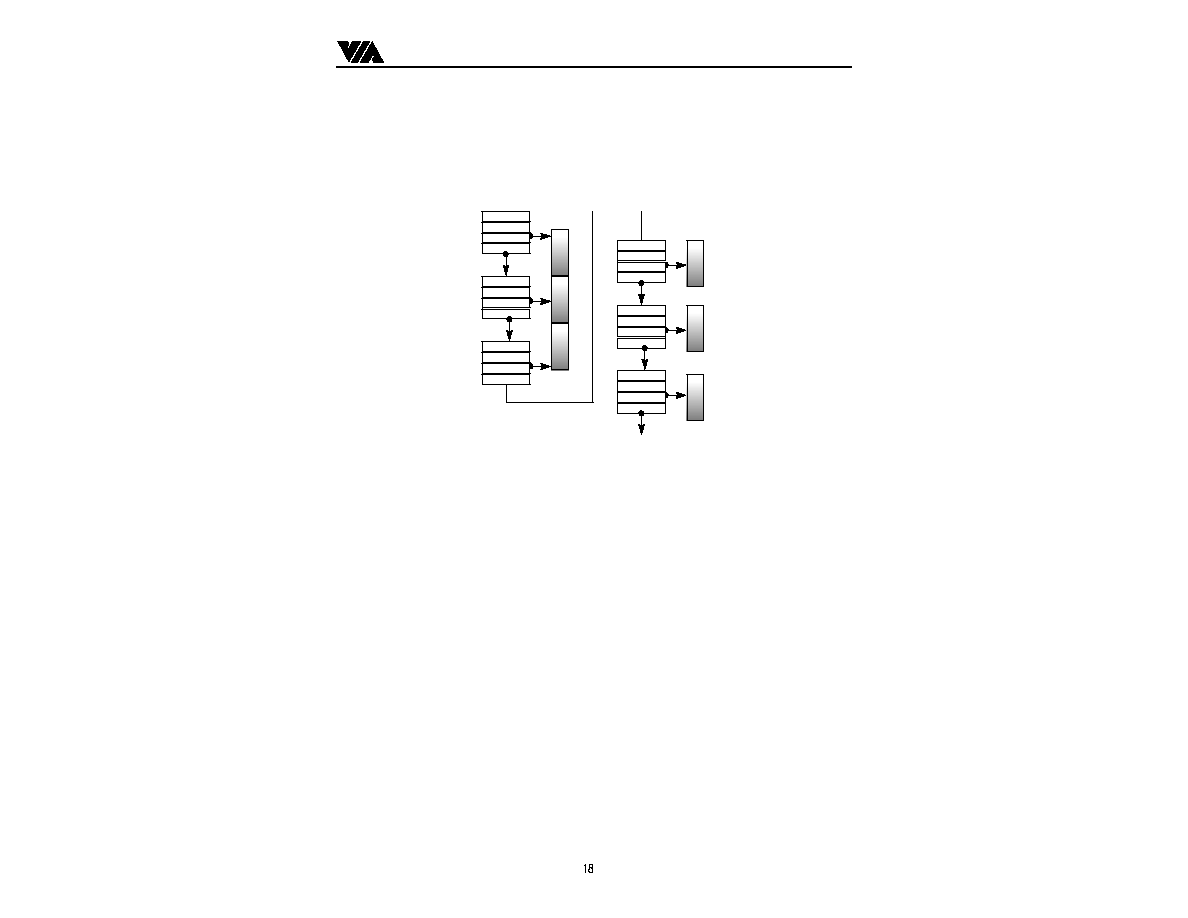
Figure 6-1 VT86C100A Buffer Management : Chain buffer Structure
6.1 D
ESCRIPTOR
R
ING AND
C
HAIN
S
TRUCTURE
6.1.1 R
ECEIVE
D
ESCRIPTORS
Figure 6-2 shows the receive descriptor format :
Providing single buffer, one byte-count buffers, and next descriptor address. And Chain bit control
span multiple data buffers data chain to be compatible various types of memory management schemes..
VIA Technologies, Inc.
Preliminary VT86C100A
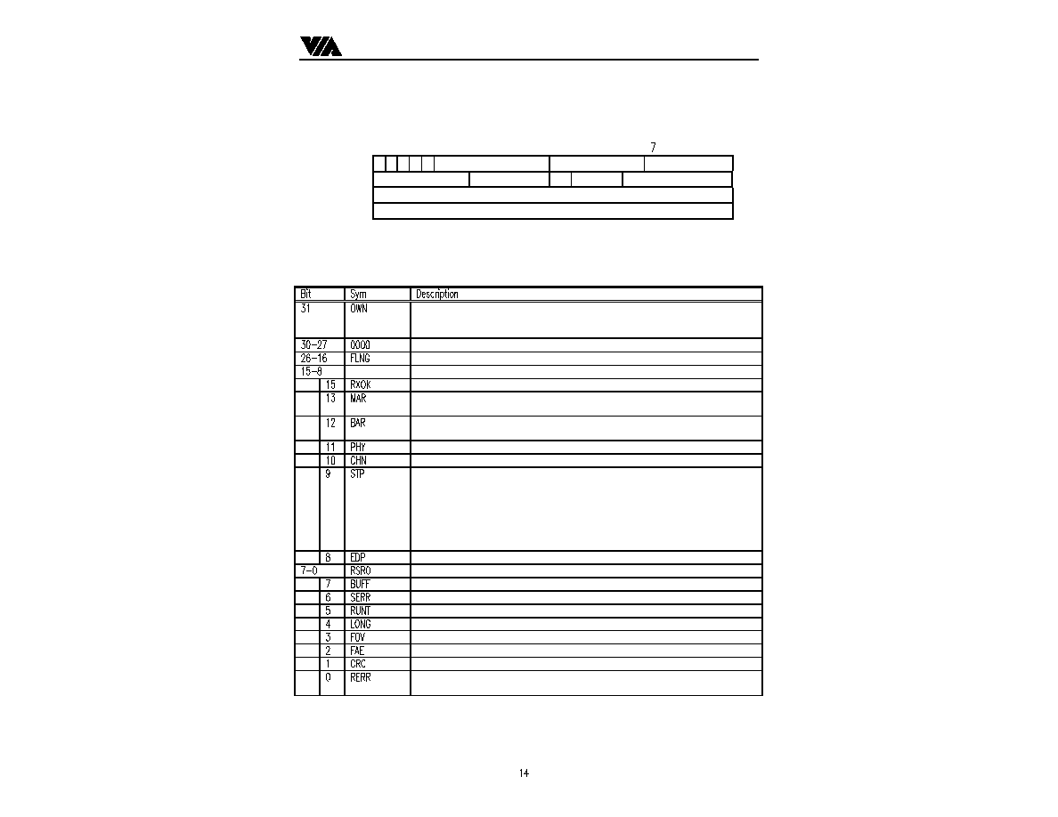
31
23
15
RDES0
O
0 0 0 0
FLNG[10:0]
RSR1
RSR0
RDES1
Reserve
Reserve
C
0000
RLNG[10:0]
RDES2
Rx Data Buffer Start Address
RDES3
Next Descriptor Address
F
IGURE
6-2
THE RECEIVE DESCRIPTOR FORMAT
:
6.1.2. R
ECEIVE
D
ESCRIPTOR
0 (RDES0)
RDES0 contain the received frame status, the frame length and the descriptor ownership information.
Owner : This bit control by driver, 1 to identify this descriptor own by
VT86C100A controller, 0 means this descriptor be a free descriptor; Driver must
set this bit be zero when initialed.
Extend Frame Length : Extend byte count for no-normal size Ethernet frame
Frame Length : Received frame length,
Received OK : The VT86C100A received a good packet from network.
Multicast Address Received : VT86C100A MAC received multicast address
packet
Boardcast Address Received : VT86C100A MAC received boardcast address
packet
Physical Address Received : Physical address received
CHAIN : means of chain buffer,
Start of Packet : In descriptor ring structure, STP=EDP=1 single buffer
descriptor, or chained buffer structure be follows :
STP EDP Description
1 1 Single buffer descriptor
1 0 First buffer descriptor, further buffer chained
0 1 Chained buffer packet end
0 0 X
End of Packet : End of Packet buffer
Receive Status Register 0 :
Buffer Error : Receive Buffer Error
System bus error :
Runt Packet Received :
Long Packet Received :
FIFO Overflow :
Frame Align Error :
CRC Error : received frame CRC checksum error
Receive Error : this bit be set by CRC error or frame alignmnet error or FIFO
overflow or System bus error.
VIA Technologies, Inc.
Preliminary VT86C100A
6.1.3. R
ECEIVE
D
ESCRIPTOR
1 (RDES1)
RDES1 contain the interrupt control enable, the chained frame identical and the receive buffer
fragment size information.
Interrupt Control : This bit support for interrupt PACEing , set 1 mean the
VT86C100A received this descriptor will generate the interrupt.
Chain : Chain buffer , this bit be set to 1 means there are chained buffer in next
descriptor
Extend Fragment of Frame Length : must be zero now.
Rx buffer Size : Receive buffer size for this descriptor, the total byte count of
whole frame will be stored in last descriptors
6.2.1. T
RANSMIT
D
ESCRIPTORS
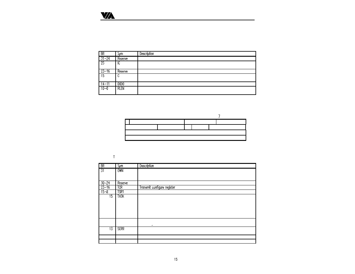
31
23
15
RDES0
O
Reserve
TSR1
TSR0
RDES1
Reserve
TCR
C
0000
TLNG[10:0]
RDES2
Tx Data Buffer Start Address
RDES3
Next Descriptor Address
F
IGURE
6-3
THE TRANSMIT DESCRIPTOR FORMAT
6.2.2. T
RANSMIT
D
ESCRIPTOR
0 (TDES0)
DES0 contain the received frame status, the frame length and the descriptor ownership information.
Owner : This bit control by driver, 1 to identify this descriptor own by
VT86C100A controller, 0 means this descriptor be a descriptor waiting for
transmit; Driver must set this bit be zero when initialed.
Transmit Status Register 1
Transmit OK : This bit be 1 for transmission error, the transmit include
following
- internal FIFO under-flow
- excessive collision (ABT)
- late collision (OWC)
- carrier sense lost (CRS)
14
JAB
Jabber : This bit will set high if Jabber condition happens. Writing to this bit has
no effect
System Error : VT86C100A MAC experience error master abort, target abort,
parity error.
12
Reserve
11
Reserve
VIA Technologies, Inc.
Preliminary VT86C100A
10
CRS
Carrier Sense lost bit is set when the carrier is lost during the transmission of a packet.
9
OWC
Late Collisions : This bit is set when late collision occurred.
8
ABT
Transmit Abort : transmit module abort after excessive collision.
7-0
TSR0
Transmit Status Register 0
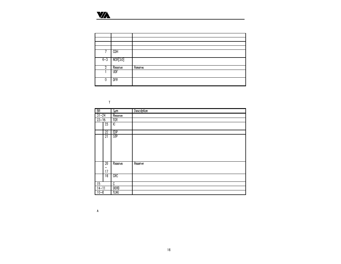
CD heartbeat : this bit only effective in 10Base-T mode. When set, this bit
indicates a heartbeat collision check failure.
Collision retry count : this 4-bits counter indicates the number of collisions that
occurred
FIFO under-flow : this bit set indicates that the transmitter aborted by transmit
FIFO encountered an empty while transmitting a frame.
Deferred: When set, indicates that the VT86C100A had to defer while ready to
transmit a frame because carrier was asserted.
6.2.3. T
RANSMIT
D
ESCRIPTOR
1 (TDES1)
DES1 contain the transmit status, the frame length and the descriptor ownership information.
Transmit Configure Register
Interrupt Control : This bit support for interrupt PACEing , set 1 mean the
VT86C100A received this descriptor will generate the interrupt.
End of Packet : End of Packet buffer
Start of Packet : In descriptor ring structure, STP=EDP=1 single buffer
descriptor, or chained buffer structure be follows :
STP EDP Description
1 1 Single buffer descriptor
1 0 First buffer descriptor, further buffer chained
0 1 Chained buffer packet end
0 0 X
CRC disable : The VT86C100A transmitter will disable generated the CRC
when this set 1.
Chain : Chain buffer
Extend Fragment of Frame Length : must be zero now.
Transmit buffer size : the fragment of frame buffer size
6.3 Buffer Structure and Interrupt Control
data consists of an entire frame or part of a frame, but it cannot exceed a single Ethernet frame size. Buffers
contain only data; All buffer status is maintained in the descriptor . Data chaining can be enable or disable by
Chain bit in DES1[15]. The interrupt control also can be enable or disable by DES1[23]
VIA Technologies, Inc.
Preliminary VT86C100A
6.3.1 Multiple Chained buffer structure
The VT86C100A can support multiple chain buffer for direct map to OS`s data buffer. The VT86C100A bus
mastering module will direct move the data from network to the OS`s data buffer or direct transmit the data in
OS`s buffer onto network not necessary move to a temperate data buffer. But the data buffer must be double
word aligned. In this multiple chained buffer structure, the first data buffer descriptor Chain
Multiple Buffer Frame
F0
C
C
0
F0
F0
Simple Ring Buffer Structure
F0
0
0
0
F1
F2
C=DES1[15]
Figure 6 : Ring buffer and multiple buffer structure
VIA Technologies, Inc.
Preliminary VT86C100A
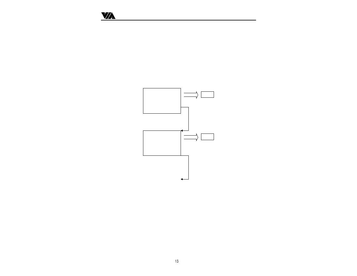
6.3.2 Interrupt Control
The VT86C100A can controllable the receive descriptors and transmit descriptor for what the interrupt
occurred.
The IC bit (DES1[23]) be set 1, the receive or transmit interrupt will be generate the interrupt no matter the
frame been complete received or transmitted. This feature will enable the OS pre-fetch the frame header or
saving the interrupt service overload.
F0
I
C
0
C
I
0
F0
F0
F1
I
C
0
C
I
0
F2
F3
ER
Interrupt
Here
Interrupt
Here
Interrupt
Here
Interrupt
Here
Save this
interrupt
Figure 7. The Interrupt Control of VT86C100A

VIA Technologies, Inc.
Preliminary VT86C100A
VT86C100A R
EGISTERS
Group 1 : Internal Command Status Register (CSR) Layout
NO
byte3
byte2
byte1
byte0
type
00
PAR3/KEY3
PAR2/KEY2
PAR1/KEY1
PAR0/KEY0
RW
04
TCR
RCR
PAR5/KEY5
PAR4/KEY4
RW
08
CR1
CR0
RW
0c
IMR2
IMR0
ISR1
ISR0
RW
10
MAR3
MAR2
MAR1
MAR0
RW
14
MAR7
MAR6
MAR5
MAR4
RW
18
Curr Rx Desc Addr
RW
1c
Curr Tx Desc Addr
RW
20
Current Rx Desc 0
RO
24
Current Rx Desc 1
RO
28
Current Rx Desc 2
RO
2c
Current Rx Desc 3
RO
30
Next Rx Desc 0
RO
34
Next Rx Desc 1
RO
38
Next Rx Desc 2
RO
3c
Next Rx Desc 3
RO
40
Current Tx Desc 0
RO
44
Current Tx Desc 1
RO
48
Current Tx Desc 2
RO
4c
Current Tx Desc 3
RO
50
Next Tx Desc 0
RO
54
Next Tx Desc 1
RO
58
Next Tx Desc 2
RO
5c
Next Tx Desc 3
RO
60
Current Rx DMA Pointer
RW
64
Current Tx DMA Pointer
RW
68
Tally counter test port
RW
6c
BCR1
BCR0
MIISR
PHY ADR
70
MII DATA REG
MIIADR
MIICR
RW
74
GPIO
TEST
EECSR
RW
78
CFGD
CFGC
CFGB
CFGA
RW
7c
Tally counter_CRC
Tally counter_MPA
RW
VIA Technologies, Inc.
Preliminary VT86C100A
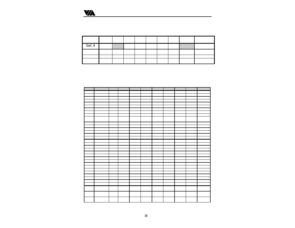
Configuration and Diagnostic Registers
Register
Bit 7
Bit 6
Bit 5
Bit 4
Bit 3
Bit 2
Bit 1
Bit 0
Read/
Write
EELOAD
JUMPE
R
MMIOE
N
MIIOPT
AUTO
OPT
MT10E
NI
MT10E
NO
MT10EOE
78H
Conf. B
QPKTDIS
TPACE
N
MRDM
TXARB
IT
RXARB
IT
MWW
AIT
MRWA
IT
LATMEM
79H
Conf. C
RES
BROPT
DLYEN
DTSEL
BTSEL
BPS2
BPS1
BPS0
7AH
Conf. D
GPIOEN
DIAG
MRDL
EN
MAGIC
CRAD
OM
CAP
MBA
BAKOPT
7BH
Note :
1.
The shaded area denoted that those bits are also selective via external jumpers.
2.
All reserved bit must be zero.
No.
Name
Type
Bit 7
Bit 6
Bit 5
Bit 4
Bit 3
Bit 2
Bit 1
Bit 0
00H
PAR0
R/W
DA7
DA6
DA5
DA4
DA3
DA2
DA1
DA0
01H
PAR1
R/W
DA15
DA14
DA13
DA12
DA11
DA10
DA9
DA8
02H
PAR2
R/W
DA9
DA10
DA11
DA12
DA13
DA14
DA15
DA16
03H
PAR3
R/W
DA17
DA18
DA19
DA20
DA21
DA22
DA23
DA24
04H
PAR4
R/W
DA25
DA26
DA27
DA28
DA29
DA30
DA31
DA32
05H
PAR5
R/W
DA33
DA34
DA35
DA36
DA37
DA38
DA39
DA40
06H
RCR
R/W
RRFT2
RFT1
RFT0
PROM
AB
AM
AR
SEP
07H
TCR
R/W
RTSF
RTFT1
RTFT0
OFST
LB1
LB0
08H
CR0
R/W
RDMD
TDMD
TXON
RXON
STOP
STRT
INIT
09H
CR1
R/W
SRST
RDMD1
TDMD1
KEYPA
G
DPOLL
FDX
ETEN
EREN
0AH
0BH
0CH
ISR0
R/W
CNT
BE
RU
TU
TXE
RXE
PTX
PRX
0DH
ISR1
R/W
KEYI
SRCI
ABTI
NBFI
PRAI
OVFI
ETI
ERI
0EH
IMR0
R/W
CNTM
BEM
RUM
TUM
TXEM
RXEM
PTXM
PRXM
0FH
IMR1
R/W
KEYIM
SRCM
ABTM
NBFM
PRAIM
OVFM
ETM
ERM
10H
MAR0
R/W
FB7
FB6
FB5
FB4
FB3
FB2
FB1
FB0
11H
MAR1
R/W
FB15
FB14
FB13
FB12
FB11
FB10
FB9
FB8
12H
MAR2
R/W
FB23
FB22
FB21
FB20
FB19
FB18
FB17
FB16
13H
MAR3
R/W
FB31
FB30
FB29
FB28
FB27
FB26
FB25
FB24
14H
MAR4
R/W
FB39
FB38
FB37
FB36
FB35
FB34
FB33
FB32
15H
MAR5
R/W
FB47
FB46
FB45
FB44
FB43
FB42
FB41
FB40
16H
MAR6
R/W
FB55
FB54
FB53
FB52
FB51
FB50
FB49
FB48
17H
MAR7
R/W
FB63
FB62
FB61
FB60
FB59
FB58
FB57
FB56
18H
RDA0
R/W
AB7
AB6
AB5
AB4
AB3
AB2
AB1
AB0
19H
RDA1
R/W
AB15
AB14
AB13
AB12
AB11
AB10
AB9
AB8
1AH
RDA2
R/W
AB23
AB22
AB21
AB20
AB19
AB18
AB17
AB16
1BH
RDA3
R/W
AB31
AB30
AB29
AB28
AB27
AB26
AB25
AB24
1CH
TDA0
R/W
AB7
AB6
AB5
AB4
AB3
AB2
AB1
AB0
1DH
TDA1
R/W
AB15
AB14
AB13
AB12
AB11
AB10
AB9
AB8
1EH
TDA2
R/W
AB23
AB22
AB21
AB20
AB19
AB18
AB17
AB16
1FH
TDA3
R/W
AB31
AB30
AB29
AB28
AB27
AB26
AB25
AB24
6CH
MPHY
R/W
MPO1
MPO0
PHYAD
4
PHYAD
3
PHYAD
2
PHYAD
1
PHYAD0
6DH
MIISR
R/W
GPIO1P
OL
LEDPO
L
MFDC
PHYOP
T
MIIERR
MRERR
LNKFL
SPEED
6EH
BCR0
R/W
REQOP
T
CRFT2
CRFT1
CRFT0
DMAL2
DMAL1
DMAL0
VIA Technologies, Inc.
Preliminary VT86C100A
6FH
BCR1
R/W
CTSF
CTF1
CTF0
POT2
POT1
POT0
70H
MIICR
R/W
MAUT
O
RCMD
WCMD
MDPM
MOUT
MDO
MDI
MDC
71H
MIIAD
R/W
MSRCE
N
MDON
E
MAD4
MAD3
MAD2
MAD1
MAD0
72H
73H
74H
EECSR
R/W
EEPR
EMBP
LOAD
DPM
ECS
ECK
EDI
EDO
75H
TEST
R/W
HBDIS
FCOL
BKOFF
TSTOV
F
TSTUD
F
TEST2
TEST1
TEST0
76H
77H
78H
CFGA
R/W
EELOA
D
JUMPE
R
MMIOE
N
MIIOPT
AUTOO
PT
MT10E
NO
MT10E
NO
MT10EO
E
79H
CFGB
R/W
QPKTD
IS
TPACE
N
MRDM
TXARB
IT
RXARB
IT
MWWA
IT
MRWAI
T
LATMEN
7AH
CFGC
R/W
BROPT
DLYEN
DTSEL
BTSEL
BPS2
BPS1
BPS0
7BH
CFGD
R/W
GPIOE
N
DIAG
MRDLE
N
MAGIC
CRADO
M
CAP
MBA
BAKOPT
7CH
MPAC0
R/W
CD7
CD6
CD5
CD4
CD3
CD2
CD1
CD0
7DH
MPAC1
R/W
CD15
CD14
CD13
CD12
CD11
CD10
CD9
CD8
7EH
CRCC0
R/W
CD7
CD6
CD5
CD4
CD3
CD2
CD1
CD0
7FH
CRCC1
R/W
CD15
CD14
CD13
CD12
CD11
CD10
CD9
CD8
VIA Technologies, Inc.
Preliminary VT86C100A
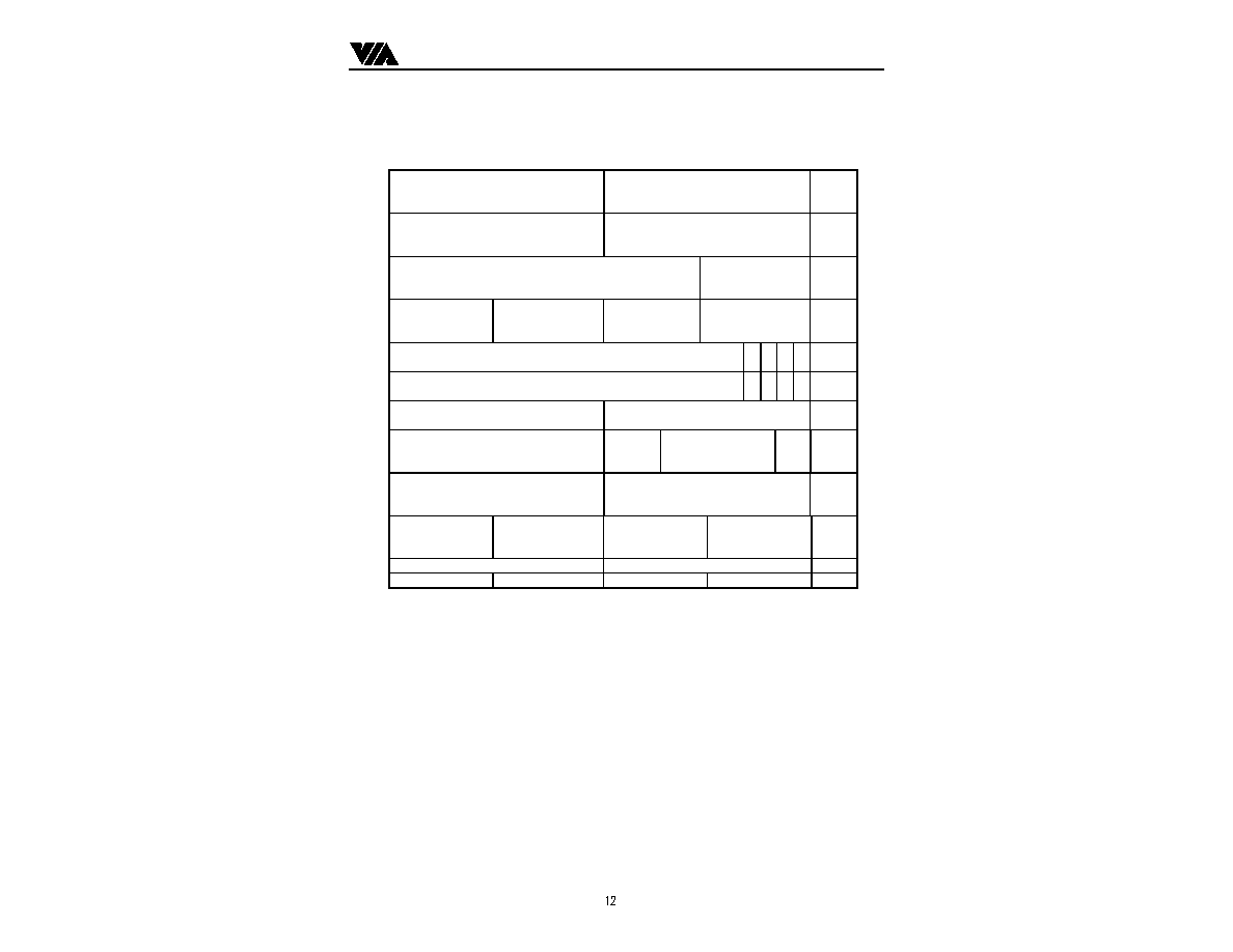
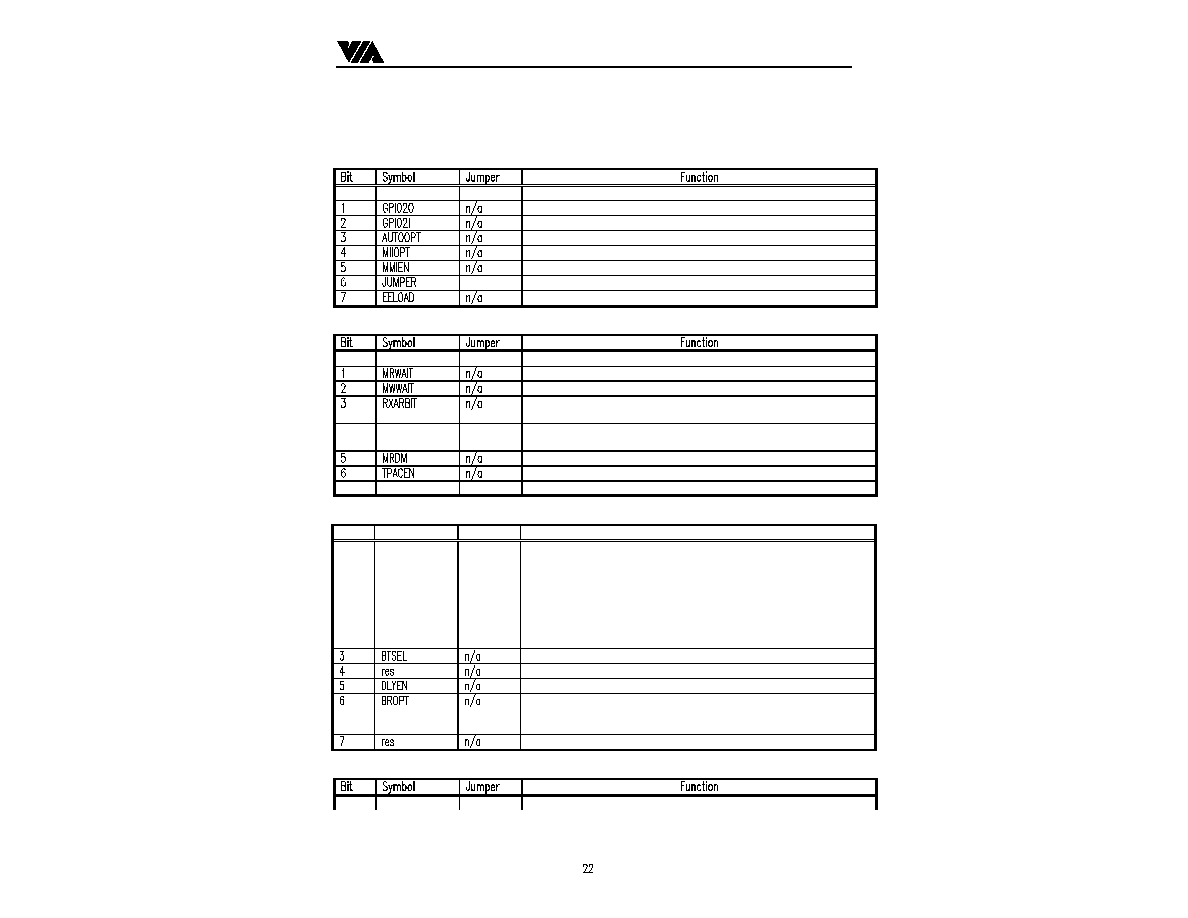
1.1 Configure Register Layout
Configuration Register A (0x78)
0
GPIO2OE
MD3
GPIO2OE : Output enable of GPIO2 pin
GPIO2O : Output to GPIO2 pin
GPIO2I : GPIO2 input status
AUTOOPT : enable receive event auto transmit descriptor polling
MMIEN : Memory mapped IO enable, accept memory command
GPIO2
JUMPER : Jumper mode to select PHY and operation mode
EELOAD : Enable EEPROM embedded and direct programming
Configuration Register B (0x79)
0
LATMEN
n/a
LATMEN: Latency timer effect enable
MRWAIT : Master read insert one wait state 2-2-2-2
MWWAIT: Master write insert one wait state 2-2-2-2
RXARBIT : the receiving FIFO DMA will be interleave to transmitting
FIFO DMA after 32 double words transaction.
4
TXARBIT
n/a
TXARBIT : the transmitting FIFO DMA will be interleave to receiving
FIFO DMA after 32 double words transaction.
MRDM : Memory read multiple capable
TPACEN : Tx descriptor pacing algorithm enable
7
QPKTDIS
n/a
QPKTDIS : disable transmit frame queuing.
Configuration Register C (0x7A)
Bit
Symbol
Jumper
Function
0-2
BPS0-
BPS3
n/a
Boot PROM Select: Select size at which boot PROM begins and the
size
Bit2
Bit1
Bit0
Size
0
0
0
No Boot PROM
0
0
1
8K
0
1
0
16K
0
1
1
32K
1
X X
64K
BTSEL : Bootrom timing select
DLYEN : Delay transaction while memory read Bootrom
BROPT : set Bootrom address line above Bootrom size selected to logic
1
for small size Bootrom
Configuration Register D (0x7B)
0
BAKOPT
n/a
BAKOPT : Back-off algorithm optional
VIA Technologies, Inc.
Preliminary VT86C100A
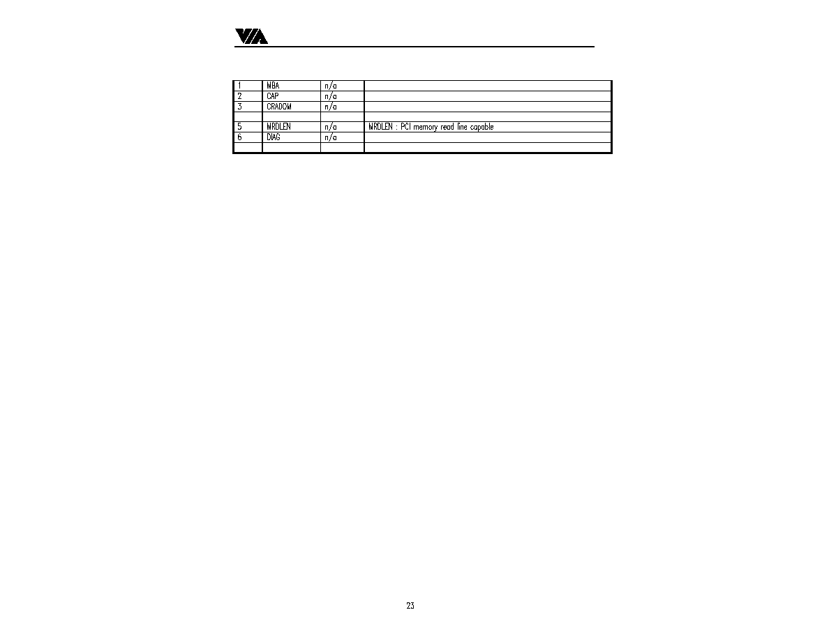
MBA : Modify back off algorithm
CAP : Capture effect back off
CRADOM : Random back off algorithm
4
MAGIC
n/a
MAGIC : Turn on Magic key
DIAG :
7
GPIOEN
n/a
GPIOEN : Turn on GPIO2 input status change monitor
VIA Technologies, Inc.
Preliminary VT86C100A
VT86C100A Command Status Registers
MAC command and status register Group
CR0:
Command Register 0 (08H; Type=R/W)
This register is used to select register pages, enable or disable remote DMA operation and issue
commands.
Reserved
6
RDMD
This bit indicates that the VT86C100A receive poll demand enable
5
TDMD
This bit indicates that the VT86C100A transmit poll demand enable
4
TXON
This bit indicates that the VT86C100A start transmit state while STRT bit on
3
RXON
This bit indicates that the VT86C100A start receive state while STRT bit on
2
STOP
This bit indicates that the VT86C100A into STOP state , this bit set by SFRST bit or
hardware reset
1
STRT
This bit indicates that VT86C100A enter the start command.
0
INIT
Initialize Start : When set on the VT86C100A start to set its bus master register the start
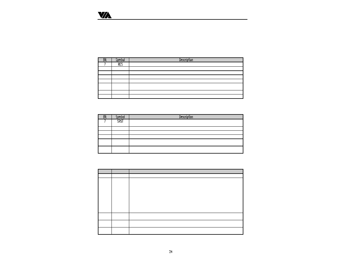
CR1:
Command Register 1 (09H; Type=R/W)
This register is used to select register pages, enable or disable remote DMA operation and issue
commands.
This bit is set when VT86C100A enters reset state and is cleared when a start command is
issued to the CR1. It is also set when receive buffer overflows or system error.
6-4
RES
Reserved
3
DPOLL
Disable transmit auto polling
2
FDX
This bit set MAC to full duplex in 10BaseT or 100BaseT mode
1
ETEN
Early transmit mode enable while CFGD[1] be enable, this bit be clear while hardware
reset only
0
EREN
Early receive mode enable while CFGD[0] be enable, this bit be clear while hardware reset
only
RCR:
Receive Configuration Register (06H; Type=R/W)
This register reflects the NIC receive configuration and reset by hardware reset and software reset
Bit
Symbol
Description
7
RRSF
Receive store and forward
6-5
RFT[1-0]
Receive FIFO Threshold.
RRFT2 RRFT1 RRFT0 Threshold
0 0 0 64 bytes
0 0 1 32
0 1 0 128
0 1 1 256
1 0 0 512
1 0 1 768
1 1 0 1024
1 1 1 Receive store and forward
4
PRO
If PRO=1, all packets with physical destination address are accepted. If PRO=0, physical
address must match the node address programmed in PAR0-5
3
AB
If AB=1, packets with broadcast destination address are accepted. If AM=0, packets with
broadcast destination are rejected.
2
AM
If AM=1, packets with multicast destination address are accepted. If AM=0, packets with
multicast destination are rejected.
VIA Technologies, Inc.
Preliminary VT86C100A
1
AR
If AR=1, packets smaller than 64 bytes are accepted. If AR=0, packets smaller than 64 are
rejected.
0
SEP
If SEP=1, packets with receive errors are accepted. If SEP=0, packets with receive errors
are rejected.
TCR: Transmit Configuration Registers (07H, Type=R/W)
Bit
Symbol
Description
7
RTSF
Transmit and store and forward : till whole packet enter into FIFO then start transmit
6-5
RFT[1-0]
Transmit FIFO Threshold :
RTSF RTF1 RTF0 Threshold
0 0 0 64 bytes
0 0 1 32
0 1 0 128
0 1 1 256
1 0 0 512
1 0 1 768
1 1 0 1024
1 1 1 Transmit store and forward
4
-
Reserve
3
OFSET
Back-off priority selection : change the back off algorithm as National specification
2-1
LB[1-0]
Loopback mode select for transmit :
0 0 Normal
0 1 Internal loopback
1 0 ENDEC loopback for 10Base-T or MII loopback
1 1 223 loopback or others
0
-
Reserved.
VIA Technologies, Inc.
Preliminary VT86C100A
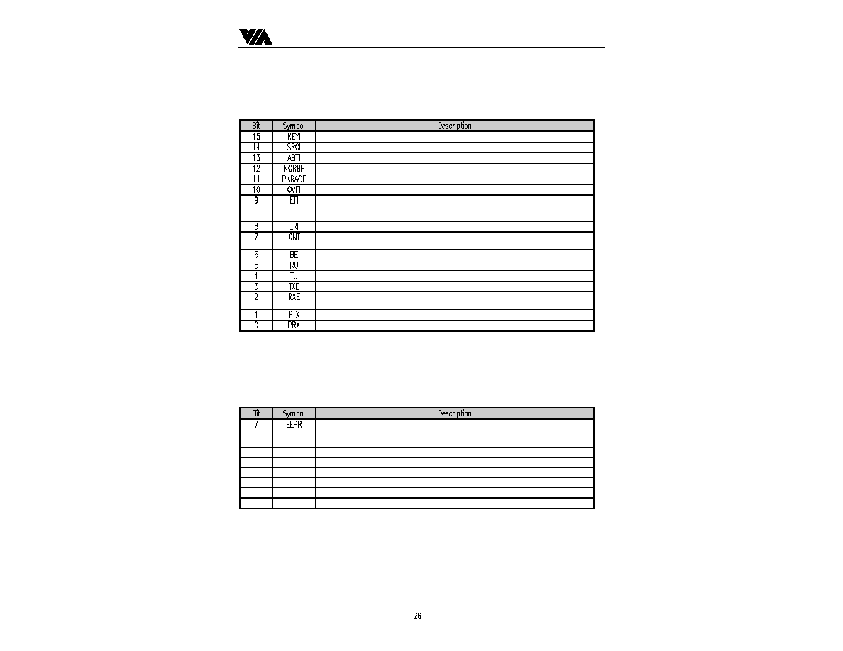
ISR:
Interrupt Status Register (0CH; Type=R/W)
This register reflects the NIC status. The host reads it to determine the cause of the interrupt
Individual bits are cleared by writing a "1" to the corresponding bit. It must be cleared after
power up.
Magic packet key received interrupt status
Port status change interrupt status
transmit abort interrupt status, this bit will be set while excessive collision
No more receive buffer to use
FIFO overflow condition, next packet race into FIFO with current packet
receiving FIFO overflow interrupt status
Transmit descriptor underflow while in early transmit mode or general I/O pin M10TENI
status change interrupt while GPIOEN=1, this interrupt can be used as PHY report the
link status change.
Indicates the received packet has filled the first data buffer.
CRC error or packet race tally counter overflow interrupt, software can maintain drivers
CRC error counter above 32 bit
PCI Bus error interrupt
Receive buffer unavailable
Transmit buffer underflow
Transmit error bit is set when a packet transmission is aborted due to excessive collisions.
This bit is set when a packet is received with one or more of the following errors:
1) CRC error, 2) Frame alignment error and 3) Missed packet.
This bit indicates that packet is transmitted with no errors.
This bit indicates that packet is received with no errors.
IMR
Interrupt Mask Register (0EH; Type=R/W )
All bits correspond to the bits in the ISR register. Power up=all 0s. Setting individual bits will
enable the corresponding interrupts.
EEPROM Configuration and status Register Group
EECSR EEPROM Command Status Register (74H, Type=R/W)
EEPROM programming status
6
EMBP
EEPROM embedded program enable, the VT86C100A will set this bit to zero after
programming complete.
5
LOAD
Dynamic reload EEPROM content, the PAR[5-0] will be update
4
DPM
Direct program EEPROM
3
ECS
EEPROM interface chip select status
2
ECK
EEPROM interface clock status
1
EDI
EEPROM interface data in status
0
EDO
EEPROM interface data out status
VIA Technologies, Inc.
Preliminary VT86C100A
MII port control and status Register Group
MIICR MII interface control register (070H, Type=R/W)
MII management port auto polling enable, MIICR has no effect while this set on
6
RCMD
read enable to read PHY status, reset while complete and PHY status will be store in
register MII data register 0x72
5
WCMD
write enable to program PHY, reset while PHY programmed completely
4
MDPM
direct program mode enable, while MDPM be set , the WCMD and RCMD have no effect
3
MOUT
MDIO output enable indicator while direct program mode
2
MDO
MII interface management port data output status
1
MDI
MII interface management port data input status
0
MDC
MII interface management port clock status
MIIAD MII CSR offset address register (071H, Type=R/W)
6
MSRCE
N
5
MDONE
4
MAD4
MII management port address bit 4
3
MAD3
MII management port address bit 3
2
MAD2
MII management port address bit 2
1
MAD1
MII management port address bit 1
0
MAD0
MII management port address bit 0
The MII management port address default value be (00001)b,
MIISR MII status register (06dH, Type=R/W)
GPIO1POL : General purpose I/O 1 pin output polarity, when this bit set as '1', the
GPIO1 pin output active high; set as '0', the GPIO1 pin output active low.
6
res
Reserve
5
MFDC
MFDC : Accelerate the MDC speed when VT86C100A enter MII auto polling; MFDC set
as '0', MDC be normal speed; or MFDC set as '1' , MDC be 4 times speed.
4
PHYOPT
PHYOPT : set 1 use default external PHY device address as 0001
3
MIIERR
MIIERR : PHY device coding error by insert RX_ERR, write to clear it.
2
MRERR
MRERR : MII Management read error, write to clear it
1
LNKFL
LNKFL : Link fail in 10 or 100MHz
0
SPEED
SPEED : Network speed, 0 as 100MHZ, 1 as 10MHz
PHYADR
MII configuration register (06cH, Type=R/W)
VIA Technologies, Inc.
Preliminary VT86C100A
MII management port polling timer interval, timer unit be MDC clock cycle
MPO1 MPO0 clock
0 0 1024
0 1 512
1 0 128
1 1 64
5
res
4-0
PHYAD[
4-0]
PHY[4-0] : external PHY device address , these register bytes stored from EEPROM
loading when power up or EEPROM auto-reloading or can be programmed by software,
default as (00001)b

VIA Technologies, Inc.
Preliminary VT86C100A
[This page left to blank]
VIA Technologies, Inc.
Preliminary VT86C100A
VT5134A
A
VT3043E Bench Board
VIA TECHNOLOGIES, INC.
C
1
3
Thursday, September 04, 1997
Title
Size
Document Number
Rev
Date:
Sheet
of
EECS
MCRS
MCOL
MTXD3
MTXD2
MTXD1
MTXD0
MTXEN
MTXCK
MRXER
MRXCK
MRXDV
MRXD0
MRXD1
MRXD2
MRXD3
MDC
MDIO
M10TEN
PRTENL
PRTENH
TST
NC2
NC
HDRST
-BPRD
-PCIRST
MA[15:0]
MD[7:0]
-PME
|LINK
|2.SCH
1
3
5
7
9
11
13
15
17
19
21
23
25
27
29
31
33
35
37
2
4
6
8
10
12
14
16
18
20
22
24
26
28
30
32
34
36
38
39
41
43
45
47
49
51
53
55
57
59
61
63
65
67
69
71
73
75
77
79
81
83
85
87
89
91
93
95
97
99
101
103
105
107
109
111
113
115
117
119
121
123
125
127
40
42
44
46
48
50
52
54
56
58
60
62
64
66
68
70
72
74
76
78
80
82
84
86
88
90
92
94
96
98
100
102
104
106
108
110
112
114
116
118
120
122
124
126
128
|3.SCH
PCIVCC
AD25
AD24
-CBE3
IDSEL
AD23
AD22
AD21
AD20
AD19
AD18
AD17
AD16
-CBE2
-FRAME
-IRDY
-TRDY
-DEVSEL
-STOP
-PERR
AD31
MCRS
PAR
-CBE1
AD30
MCOL
AD15
AD14
AD29
MTXD3
AD13
AD12
PCIVCC
PCIVCC
AD28
MTXD2
AD11
AD10
-INTA
AD27
MTXD1
AD26
MTXD0
AD9
AD8
AD25
MTXEN
-CBE0
AD7
-PRSNT1
AD24
MTXCK
AD23
MRXER
-PRSNT2
AD22
MRDCK
AD21
MRXDV
AD20
MRXD0
AD6
AD5
AD19
MRXD1
AD4
-PCIRST
AD18
MRXD2
AD3
AD2
PCICLK
PCIVCC
AD17
MRXD3
AD1
AD0
-GNT
AD16
MDC
-REQ
AD15
MDIO
EECS
-BPRD
PCIVCC
-PME
AD14
MD0
MD1
AD31
AD30
AD13
M10TEN
MD2
MD3
AD29
AD12
PRTENL
MD4
AD28
AD11
PRTENH
MD5
AD27
AD26
AD10
MD6
MD7
AD25
AD9
MA15
PRTENL
PRTENH
AD24
AD8
MA14
MA0
MA1
-CBE3
IDSEL
AD7
MA13
AD23
AD6
MA12
AD22
AD5
MA11
AD21
AD20
AD4
MA10
AD19
AD3
MA9
AD18
AD2
MA8
MA2
MA3
AD17
AD16
AD1
MA7
MA4
MA5
-CBE2
AD0
MA6
MA6
MA7
-FRAME
MA5
MA8
SVDD
-IRDY
-CBE3
MA4
SVSS
-TRDY
-CBE2
MA3
MA9
-DEVSEL
-CBE1
MA2
MA10
MA11
-STOP
-CBE0
MA1
MA12
MA13
MA0
MA14
MA15
-PERR
IDSEL
NC
NC2
-FRAME
MD7
-IRDY
MD6
TST
MCRS
PAR
-TRDY
MD5
MCOL
MTXD3
-CBE1
AD15
-DEVSEL
MD4
MTXD2
MTXD1
AD14
-STOP
MD3
MTXD0
MTXEN
AD13
PAR
MD2
AD12
AD11
PCICLK
MD1
MTXCK
MRXER
AD10
-INTA
MD0
MRXCK
MRXDV
AD9
-PCIRST
-GNT
EECS
-REQ
-BPRD
AD8
-CBE0
-PERR
AD7
-PME
TST
MRXD0
MRXD1
AD6
NC2
MRXD2
MRXD3
AD5
AD4
NC
AD3
MDC
MDIO
AD2
HDRST
HDRST
M10TEN
AD1
AD0
-INTA
-PCIRST
PCIVCC
PCIVCC
PCICLK
SVDD
-GNT
-REQ
-PME
AD31
AD30
AD29
AD28
SVSS
AD27
AD26
MA[15:0]
MD[7:0]
C1
.1u
C2
.1u
C3
.1u
C4
.1u
C5
.1u
C6
.1u
C7
.1u
JP1
HEADER 72X2
1
3
5
7
9
11
13
15
17
19
21
23
25
27
29
31
33
35
37
39
41
43
45
47
49
51
53
55
57
59
61
63
65
67
69
71
73
75
77
79
81
83
85
87
89
91
93
95
97
99
101
103
105
107
109
111
113
115
117
119
121
123
125
127
129
131
133
135
137
139
141
143
2
4
6
8
10
12
14
16
18
20
22
24
26
28
30
32
34
36
38
40
42
44
46
48
50
52
54
56
58
60
62
64
66
68
70
72
74
76
78
80
82
84
86
88
90
92
94
96
98
100
102
104
106
108
110
112
114
116
118
120
122
124
126
128
130
132
134
136
138
140
142
144
U1
VT3043E
AD30
122
AD29
123
AD28
124
AD27
127
AD26
128
AD25
1
AD24
2
AD23
5
AD22
7
AD21
8
AD20
9
AD19
11
AD18
12
AD17
13
AD16
14
AD15
27
AD14
28
AD13
29
AD12
30
AD11
31
AD10
32
AD9
35
AD8
36
AD7
38
AD6
39
AD5
40
AD4
42
AD3
43
AD2
44
AD0
46
CBE3
3
AD1
45
CBE2
16
CBE1
26
CBE0
37
IDSEL
4
FRAME
17
IRDY
18
TRDY
19
DEVSEL
20
STOP
21
PAR
25
PCICLK
115
INTA
113
PCIRST
114
GNT
118
REQ
119
PERR
23
AD31
121
VDD
10
VDD
22
VDD
34
VDD
47
VDD
56
SVDD
74
SVSS
75
PRTENH
62
PRTENL
61
MD7
60
MD6
59
MD5
58
MD4
55
MD3
54
MD2/EECK
53
MD1/EEDI
52
MD0/EEDO
51
MA15
84
MA14
83
MA13
82
MA12
81
MA11
80
MA10
79
MA9
78
MA8
73
MA7
72
MA6
71
MA5
70
MA4
69
MA3
68
MA2
67
MA1
64
MA0
63
MDIO
110
M10TEN
112
VSS
6
VSS
15
VSS
24
VSS
33
VSS
41
VSS
48
EECS
49
BPRD
50
VDD
65
VDD
76
VDD
87
VSS
57
VSS
66
VSS
77
VSS
88
VSS
98
MCRS
90
MCOL
91
MTXD3
92
MTXD2
93
MTXD1
94
MTXD0
95
MTXE
96
MTXC
99
MERR
100
MRXC
101
MRXDV
102
MRXD0
103
HDRST
111
MRXD2
105
MRXD1
104
MDC
109
MRXD3
106
PME
120
NC
85
NC2
86
TST
89
VDD
97
VSS
107
VDD
108
VSS
116
VDD
117
VDD
125
VSS
126
R1
0
C8
.1u
C9
10uF
C10
.O1u
R2
3.6
0805
C11
.1u
C12
.1u
C13
.1u
C14
.1u
C15
.1u
P1
PCI_CONA
A1
1
A2
2
A3
3
A4
4
A5
5
A6
6
A7
7
A8
8
A9
9
A10
10
A11
11
A12
12
A13
13
A14
14
A15
15
A16
16
A17
17
A18
18
A19
19
A20
20
A21
21
A22
22
A23
23
A24
24
A25
25
A26
26
A27
27
A28
28
A29
29
A30
30
A31
31
A32
32
A33
33
A34
34
A35
35
A36
36
A37
37
A38
38
A39
39
A40
40
A41
41
A42
42
A43
43
A44
44
A45
45
A46
46
A47
47
A48
48
A49
49
A52
52
A53
53
A54
54
A55
55
A56
56
A57
57
A58
58
A59
59
A60
60
A61
61
A62
62
P2
PCI_CONB
B1
1
B2
2
B3
3
B4
4
B5
5
B6
6
B7
7
B8
8
B9
9
B10
10
B11
11
B12
12
B13
13
B14
14
B15
15
B16
16
B17
17
B18
18
B19
19
B20
20
B21
21
B22
22
B23
23
B24
24
B25
25
B26
26
B27
27
B28
28
B29
29
B30
30
B31
31
B32
32
B33
33
B34
34
B35
35
B36
36
B37
37
B38
38
B39
39
B40
40
B41
41
B42
42
B43
43
B44
44
B45
45
B46
46
B47
47
B48
48
B49
49
B52
52
B53
53
B54
54
B55
55
B56
56
B57
57
B58
58
B59
59
B60
60
B61
61
B62
62
R3
0
R4
0
R5
0
R6
0
R7
0
R8
0
CB1
22UF
CB2
22UF
CB3
22UF
CB4
22UF
CB5
22UF
CB8
22UF
CB7
22UF
VIA Technologies, Inc.
Preliminary VT86C100A
VT5134A
A
NS or Myson's PHY & Transceiver
VIA TECHNOLOGIES, INC.
C
2
3
Thursday, September 04, 1997
Title
Size
Document Number
Rev
Date:
Sheet
of
MTD972
NS 840
R22
R24
R23
V
V
V
OSC2
50M
25M
'*' for Myson PHY and Transceiver
R42
V
*Use RP1,RP2 or Only RP2 -> 510
SPEED10
TX_ER
TXO+/TXU+
MII_CRS
TXU-
TXO-
RXI+
RXI-
PUD01
MII_RXER
PTD+
PTD-
MDC
TXO+/TXU+
MDIO
PRD+
TXO-
PRD-
RESET
RXI+
PSD+
RXI-
REFIN
PSD-
CLK25
OSCIN
P1
P0
P3/100
AN0
SPEED10
AN1
RXI+
PUD02
RXI-
OSCIN
TXO+/TXU+
TXU-
P3/100
TXO-
PUD03
REFIN
CLK25
ANAVCC
FGND
TX_ER
RESET
PUD01
AN0
PUD03
P0
PRD+
PRD-
PSD-
PUD01
PSD+
P1
PTD-
AN1
PUD02
PTD+
ANAVCC
PUD03
MII_CRS
P3/100
MII_RXER
C16
.001u
R9
10K
U2
DP83223
Transceiver
TXO+
9
TXO-
8
RXI+
2
RXI-
1
PMRD+
15
PMRD-
16
PMID+
25
PMID-
24
SD+
20
SD-
21
ENCSEL
12
LBEN
19
TXREF
6
TXVCC
5
TXVCC
11
RXVCC
4
RXVCC
27
TXGND
7
TXGND
10
RXGND
3
RXGND
28
EXTVCC
23
VCC
26
VCC
13
GND
14
GND
22
EQSEL
17
/CDET
18
C17
10P
C18
.1u
C19
.1u
C20
.1u
C21
.1u
C22
.1u
C23
.1u
C24
.1u
C25
.1u
C26
.1u
C27
.1u
C28
.1u
C29
.1u
C30
.1u
C31
.1u
C32
.1u
C33
.1u
R10
4.7K
C34
.1u
R11
0
R12
10
R13
10
J1
RJ-45
1
2
3
4
5
6
7
8
9
10
11
12
13
14
L1
PT4171
CT
TD+
TD-
RX+
CT
RX-
TX+
CM
TX-
RD+
1
2
3
16
14
15
7
5
6
10
12
11
R14
*2K
R15
*0
R16
*0
RN1
510
1
3
5
7
2
4
6
8
Q1
2N3904
2
3
1
Q2
2N3904
2
3
1
Q3
2N3904
2
3
1
R21
4.7K
R22
75
R23
0
R24
*75
OSC1
50MHz/*25MHz
VCC
4
OUT
3
NC
1
GND
2
CX1
.1u
R25
510
R26
4.7K
R27
75
R28
75
R29
75
R30
75
C35
.1u
R31
10
R32
*0
R33
0
C37
.1u
C38
.1u
L2
47uH
C39
.1u
C40
22u
R35
0
R36
510
R37
*0
C41
*.1u
R38
47.5
1%
R39
47.5
1%
U3
DP83840A
Physical Layer
TX_CLK
82
TXD3
75
TXD2
76
TXD1
77
TXD0
78
TX_EN
74
CRS_P2
66
COL
65
RXD3
55
RXD2
56
RXD1
57
RXD0
58
RX_CLK
62
RX_DV
64
RX_ER_P4
63
MDC
72
MDIO
67
TXU+
26
TXU-
25
TXS+
24
TXS-
23
RXI+
21
RXI-
20
TD+
17
TD-
16
RD+
5
RD-
6
SD+
8
SD-
7
SPEED_10
54
ENCSEL_P1
53
LBEN_P0
49
X1
33
X2
34
OSCIN
2
LED_TX
42
LED_RX
41
LED_LK
38
LED_P/F
37
LED_COL
36
REQ
29
RTX
28
CLK25M
81
REFIN
86
TX_ER
73
RX_EN
43
AN0
95
AN1
46
REPEATER
47
10BTSER
98
BPALIGN
99
BP4B5B
100
BPSCR
1
J_TD0
50
J_TDI
91
J_TRST
92
J_TCLK
93
J_TMS
94
RESET
44
PHYAD3
89
NC
13
NC
14
NC
83
RES_0
4
RES_0
45
RES_0
48
RES_0
90
VCC_A
96
VCC_A
39
VCC_A
51
PCSVCC_A
70
GND_A
97
GND_A
40
GND_A
52
PCSGND_A
71
VCC_B
59
VCC_B
68
VCC_B
79
REFVCC_B
84
GND_B
60
RCLKGND_B
61
GND_B
69
GND_B
80
REFGND_B
85
RXVCC_C
18
TDVCC_C
22
PLLVCC_C
31
OVCC_C
32
RXGND_C
19
TDGND_C
27
PLLGND_C
30
OGND_C
35
ANAVCC_D
9
CRMVCC_D
12
ECLVCC_D
15
CGMVCC_D
87
OSCGND_D
3
ANAGND_D
10
CRMGND_D
11
CGMGND_D
88
C42
.1u
R40
*49.9
1%
R41
*49.9
1%
R42
*10K
R43
*4.7K
R44
*4.7K
R45
*4.7K
R46
*4.7K
R47
*4.7K
D1
TX
D2
RX
D3
LK
D4
P/F
D5
COL
D6
100
R48
33
R49
33
R50
33
R51
33
RP1
82
1
2
3
4
5
6
7
RP2
130
1
2
3
4
5
6
7
R52
510
R53
510
R54
33
R55
33
R56
0
R57
*0
C43
*10p
U4A
74LS14
1
2
R58
10K
R59
10K
R60
10K
R61
10K
R62
10K
R63
4.7K
AN0
1
2
3
AN1
1
2
3
PHY0
1
2
3
PHY1
1
2
3
PHY2
1
2
3
PHY3
1
2
3
PHY4
1
2
3
R78
510
RN2
510
1
3
5
7
2
4
6
8
D9
PWR
R17
10/0
R18
10/0
R20
39/49.9
R19
39/49.9
R81
20
R82
22
R79
0/75
R80
0/75
L3
FB
L4
FB
C47
39p
C48
39p
HDRST
-PCIRST
MTXCK
MTXD3
MTXD2
MTXD1
MTXD0
MTXEN
MCRS
MCOL
MRXD3
MRXD2
MRXD1
MRXD0
MRXCK
MRXDV
MRXER
MDIO
MDC
VIA Technologies, Inc.
Preliminary VT86C100A
VT5134A
A
VT3043E Strapping
VIA TECHNOLOGIES, INC.
C
3
3
Thursday, September 04, 1997
Title
Size
Document Number
Rev
Date:
Sheet
of
EECS
MD7
-BPRD
MD6
MD5
MD4
MD3
MD2
MD1
MD0
PCI_PWR
PCI_GOOD
ISOLATE
MD1
MD0
MD2
EECS
ALTRST
AUX_PWR
MA0
MD0
MA1
MD1
MA2
MD2
MA3
MD3
MA4
MD4
MA5
MD5
MA6
MD6
MA7
MD7
MA8
MA9
MA10
MA11
MA12
MA13
MA14
MA15
-BPRD
MD[7:0]
MA[15:0]
J2
1
3
4
2
5
6
7
8
9
11
10
12
13
14
16
15
J3
1
2
3
4
5
6
7
8
RP3
10K
1
2
3
4
5
6
7
8
9
RP4
10K
1
2
3
4
5
6
7
8
9
J4
1
3
4
2
5
6
7
8
9
11
10
12
13
14
16
15
J5
1
2
3
4
5
6
7
8
RP5
4.7K
1
2
3
4
5
6
7
8
9
RP6
4.7K
1
2
3
4
5
6
7
8
9
U5
93C46
DI
3
SK
2
CS
1
DO
4
VCC
8
GND
5
U6
27512
A0
10
A1
9
A2
8
A3
7
A4
6
A5
5
A6
4
A7
3
A8
25
A9
24
A10
21
A11
23
A12
2
A13
26
A14
27
A15
1
CE
20
OE
22
O0
11
O1
12
O2
13
O3
15
O4
16
O5
17
O6
18
O7
19
R64
0
R65
0
R66
4.7K
R67
4.7K
U7
TL7705A
REF
1
RESIN
2
CT
3
GND
4
VCC
8
SENSE
7
RESET
6
RESET
5
Q4
NPN
2
3
1
D7
1N4148
D8
1N4148
TP1
1
TP2
1
TP3
1
TP4
1
TP5
1
R68
0
R69
0
R70
0
R71
10K
R72
7.8K
R73
10K
R74
10K
R75
100K
C44
100p
R76
4.7K
R77
0
C45
.1u
C46
.1u
P3
AUX5V_CON
AUX5V
1
NC
2
GND
3
WAKUP
4
GND
5
AUX5V
6
U8A
74HC14
1
2
U8B
74HC14
3
4
U8C
74HC14
5
6
U8D
74HC14
9
8
MD[7:0]
EECS
-BPRD
M10TEN
PRTENH
PRTENL
TST
NC2
MA[15:0]
NC
-PME