 | –≠–ª–µ–∫—Ç—Ä–æ–Ω–Ω—ã–π –∫–æ–º–ø–æ–Ω–µ–Ω—Ç: CNY17F | –°–∫–∞—á–∞—Ç—å:  PDF PDF  ZIP ZIP |

CNY17F
Document Number 83607
Rev. 1.5, 26-Oct-04
Vishay Semiconductors
www.vishay.com
1
1
2
3
6
5
4
NC
C
E
A
C
NC
18216
Pb
Pb-free
e3
Optocoupler, Phototransistor Output, No Base Connection
Features
∑ Breakdown Voltage, 5300 V
RMS
∑ No Base Terminal Connection for Improved Com-
mon Mode Interface Immunity
∑ Long Term Stability
∑ Industry Standard Dual-in-Line Package
∑ Lead-free component
∑ Component in accordance to RoHS 2002/95/EC
and WEEE 2002/96/EC
Agency Approvals
∑ UL1577, File No. E52744 System Code H or J,
Double Protection
∑ DIN EN 60747-5-2 (VDE0884)
DIN EN 60747-5-5 pending
∑ BSI IEC60950 IEC60065
∑ FIMKO
Description
The CNY17F is an optocoupler consisting af a Gal-
lium Arsenide infrared emitting diode optically cou-
pled to a silicon planar phototransistor detector in a
plastic plug-in DIP-6 package.
The coupling device is suitable for signal transmission
between two electrically separated circuits. The
potential difference between the circuits to be coupled
is not allowed to exceed the maximum permissible
reference voltages.
In contrast to the CNY17 Series, the base terminal of
the F type is not conected, resulting in a substantially
improved common-mode interference immunity.
Order Information
For additional information on the available options refer to
Option Information.
Part
Remarks
CNY17F-1
CTR 40 - 80 %, DIP-6
CNY17F-2
CTR 63 - 125 %, DIP-6
CNY17F-3
CTR 100 - 200 %, DIP-6
CNY17F-4
CTR 160 - 320 %, DIP-6
CNY17F-1X006
CTR 40 - 80 %, DIP-6 400 mil (option 6)
CNY17F-1X007
CTR 40 - 80 %, SMD-6 (option 7)
CNY17F-1X009
CTR 40 - 80 %, SMD-6 (option 9)
CNY17F-2X006
CTR 63 - 125 %, DIP-6 400 mil (option 6)
CNY17F-2X007
CTR 63 - 125 %, SMD-6 (option 7)
CNY17F-2X009
CTR 63 - 125 %, SMD-6 (option 9)
CNY17F-3X006
CTR 100 - 200 %, DIP-6 400 mil (option 6)
CNY17F-3X007
CTR 100 - 200 %, SMD-6 (option 7)
CNY17F-3X009
CTR 100 - 200 %, SMD-6 (option 9)
CNY17F-4X006
CTR 160 - 320 %, DIP-6 400 mil (option 6)
CNY17F-4X007
CTR 160 - 320 %, SMD-6 (option 7)
CNY17F-4X009
CTR 160 - 320 %, SMD-6 (option 9)

www.vishay.com
2
Document Number 83607
Rev. 1.5, 26-Oct-04
CNY17F
Vishay Semiconductors
Absolute Maximum Ratings
T
amb
= 25 ∞C, unless otherwise specified
Stresses in excess of the absolute Maximum Ratings can cause permanent damage to the device. Functional operation of the device is
not implied at these or any other conditions in excess of those given in the operational sections of this document. Exposure to absolute
Maximum Rating for extended periods of the time can adversely affect reliability.
Input
Output
Coupler
Parameter
Test condition
Symbol
Value
Unit
Reverse voltage
V
R
6.0
V
DC forward current
I
F
60
mA
Surge forward current
t
10 µs
I
FSM
2.5
A
Power dissipation
P
diss
100
mW
Parameter
Test condition
Symbol
Value
Unit
Collector-emitter breakdown
voltage
BV
CEO
70
V
Collector current
I
C
50
mA
t
1.0 ms
I
C
100
mA
Total power dissipation
P
diss
150
mW
Parameter
Test condition
Symbol
Value
Unit
Isolation test voltage (between
emitter and detector referred to
standard climate 23/50 DIN
50014)
V
ISO
5300
V
RMS
Creepage
7.0
mm
Clearance
7.0
mm
Isolation thickness between
emitter and detector
0.4
mm
Comparative tracking index per
DIN IEC 112/VDE 0303, part 1
175
Isolation resistance
V
IO
= 500 V
R
IO
10
11
Storage temperature range
T
stg
- 55 to + 150
∞C
Ambient temperature range
T
amb
- 55 to + 100
∞C
Junction temperature
T
j
100
∞C
Soldering temperature
max. 10 s, dip soldering:
distance to seating plane
1.5 mm
T
sld
260
∞C

CNY17F
Document Number 83607
Rev. 1.5, 26-Oct-04
Vishay Semiconductors
www.vishay.com
3
Electrical Characteristics
T
amb
= 25 ∞C, unless otherwise specified
Minimum and maximum values are testing requirements. Typical values are characteristics of the device and are the result of engineering
evaluation. Typical values are for information only and are not part of the testing requirements.
Input
Output
Coupler
Current Transfer Ratio
Current Transfer Ratio I
C
/I
F
at V
CE
= 5.0 V, 25 ∞C and Collector-Emitter Leakage Current by dash number
Parameter
Test condition
Symbol
Min
Typ.
Max
Unit
Forward voltage
I
F
= 60 mA
V
F
1.25
1.65
V
Breakdown voltage
I
R
= 10
µA
V
BR
6.0
V
Reserve current
V
R
= 6.0 V
I
R
0.01
10
µA
Capacitance
V
R
= 0 V, f = 1.0 MHz
C
O
25
pF
Thermal resistance
R
th
750
K/W
Parameter
Test condition
Symbol
Min
Typ.
Max
Unit
Collector-emitter capacitance
V
CE
= 5.0 V, f = 1.0 MHz
C
CE
5.2
pF
Base - collector capacitance
V
CE
= 5.0 V, f = 1.0 MHz
C
BC
6.5
pF
Emitter - base capacitance
V
CE
= 5.0 V, f = 1.0 MHz
C
EB
7.5
pF
Thermal resistance
R
th
500
K/W
Parameter
Test condition
Part
Symbol
Min
Typ.
Max
Unit
Saturation voltage, collector-
emitter
I
F
= 10 mA, I
C
= 2.5 mA
V
CEsat
0.25
0.4
V
Coupling capacitance
C
C
0.6
pF
Collector-emitter leakage
current
V
CE
= 10 V
CNY17F-1
I
CEO
2.0
50
nA
CNY17F-2
I
CEO
2.0
50
nA
CNY17F-3
I
CEO
5.0
100
nA
CNY17F-4
I
CEO
5.0
100
nA
Parameter
Test condition
Part
Symbol
Min
Typ.
Max
Unit
Current Transfer Ratio
I
F
= 10 mA
CNY17F-1
CTR
40
80
%
CNY17F-2
CTR
63
125
%
CNY17F-3
CTR
100
200
%
CNY17F-4
CTR
160
320
%
I
F
= 1.0 mA
CNY17F-1
CTR
13
30
%
CNY17F-2
CTR
22
45
%
CNY17F-3
CTR
34
70
%
CNY17F-4
CTR
56
90
%
www.vishay.com
4
Document Number 83607
Rev. 1.5, 26-Oct-04
CNY17F
Vishay Semiconductors
Switching Characteristics
Linear operation (without saturation)
Switching operation (with saturation)
Typical Characteristics (Tamb = 25
∞C unless otherwise specified)
Parameter
Test condition
Symbol
Min
Typ.
Max
Unit
Turn-on time
I
F
= 10 mA, V
CC
= 5.0 V,
R
L
= 75 W
t
on
3.0
µs
Rise time
I
F
= 10 mA, V
CC
= 5.0 V,
R
L
= 75 W
t
r
2.0
µs
Turn-off time
I
F
= 10 mA, V
CC
= 5.0 V,
R
L
= 75 W
t
off
2.3
µs
Fall time
I
F
= 10 mA, V
CC
= 5.0 V,
R
L
= 75 W
t
f
2.0
µs
Cut-off frequency
I
F
= 10 mA, V
CC
= 5.0 V,
R
L
= 75 W
f
CO
250
kHz
Parameter
Test condition
Part
Symbol
Min
Typ.
Max
Unit
Turn-on time
I
F
= 20 mA
CNY17F-1
t
on
3.0
µs
I
F
= 10 mA
CNY17F-2
t
on
4.2
µs
CNY17F-3
t
on
4.2
µs
I
F
= 5.0 mA
CNY17F-4
t
on
6.0
µs
Rise time
I
F
= 20 mA
CNY17F-1
t
r
2.0
µs
I
F
= 10 mA
CNY17F-2
t
r
3.0
µs
CNY17F-3
t
r
3.0
µs
I
F
= 5.0 mA
CNY17F-4
t
r
4.6
µs
Turn-off time
I
F
= 20 mA
CNY17F-1
t
off
18
µs
I
F
= 10 mA
CNY17F-2
t
off
23
µs
CNY17F-3
t
off
23
µs
I
F
= 5.0 mA
CNY17F-4
t
off
25
µs
Fall time
I
F
= 20 mA
CNY17F-1
t
f
11
µs
I
F
= 10 mA
CNY17F-2
t
f
14
µs
CNY17F-3
t
f
14
µs
I
F
= 5.0 mA
CNY17F-4
t
f
15
µs
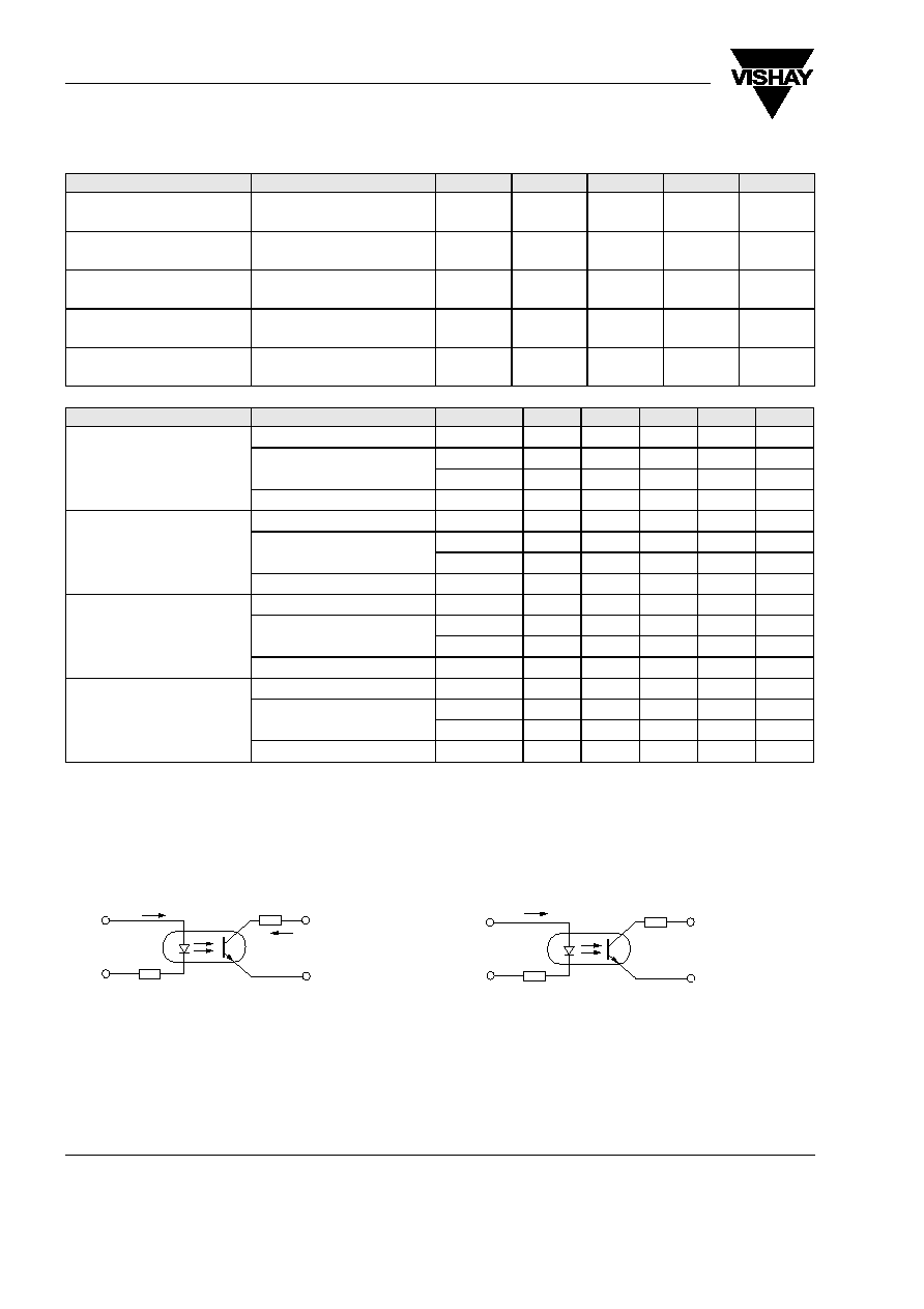
Figure 1. Linear Operation ( without Saturation)
icny17f_01
R
L
=75
V
CC
=5 V
I
C
45
I
F
Figure 2. Switching Operation (with Saturation)
I
F
1 K
V
CC
=5 V
47
icny17f_02

CNY17F
Document Number 83607
Rev. 1.5, 26-Oct-04
Vishay Semiconductors
www.vishay.com
5
Figure 3. Current Transfer Ratio vs. Diode Current
Figure 4. Current Transfer Ratio vs. Diode Current
Figure 5. Current Transfer Ratio vs. Diode Current
1
2
3
4
icny17f_03
(TA = ≠25∞C, VCE = 5.0 V)
IC/IF = f (IF)
icny17f_04
1
2
3
4
(TA = 0∞C, VCE = 5.0 V)
IC/IF = f (IF)
1
2
3
4
icny17f_05
(TA = 25∞C, VCE = 5.0 V)
IC/IF = f (IF)
Figure 6. Current Transfer Ratio vs. Diode Current
Figure 7. Current Transfer Ratio vs. Diode Current
Figure 8. Current Transfer Ratio (CTR) vs. Temperature
1
2
3
4
icny17f_06
(TA = 50∞C, VCE = 5.0 V)
A
1
2
3
4
icny17f_07
(TA = 75∞C, VCE = 5.0 V)
4
3
2
1
icny17f_08
(IF = 10 mA, VCE = 5.0 V)
IC/IF = f (T)
A