GMS05F
Vishay Semiconductors
formerly General Semiconductor
Document Number 88344
www.vishay.com
28-Feb-02
1
New Product
Surface Mount TVS Diode Array
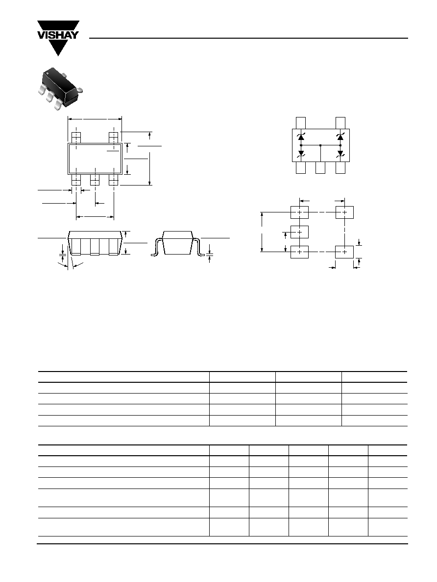
0.037 (0.95)
Ref.
0.074 (1.9)
Ref.
0.094 (2.4)
0.028 (0.7)
0.039
(1.07)
Mounting Pad Layout
Mechanical Characteristics
Case: SOT-23-5L package
Molding Compound Flammability Rating: UL 94V-0
Marking Code: F05
Packaging Codes ≠ Options:
E8 ≠ 10K per 13" reel, 30K/box
E9 ≠ 3K per 7" reel, 30K/box
Features
∑ Transient protection for data lines as per
IEC 1000-4-2 (ESD) 15kV (air), 8kV (contact)
IEC 1000-4-4 (EFT) 40A (tp = 5/50ns)
IEC 1000-4-5 (Lightning) 24A (tp = 8/20
µ
s)
∑ Small package for use in portable electronics
∑ Protects 4 I/O lines ∑ Low leakage current
∑ Low operating and clamping voltages
∑ High temperature guaranteed: 250∞C/10 sec. at terminals
Maximum Ratings and Thermal Characteristics
(T
A
= 25∞C unless otherwise noted)
Parameter
Symbol
Value
Unit
Peak Pulse Power 8/20
µ
s waveform
Ppk
350
W
Peak Pulse Current 8/20
µ
s waveform
I
PP
24
A
Operating Temperature
T
J
≠55 to +125
∞C
Storage Temperature
T
STG
≠55 to +150
∞C
Electrical Characteristics
(T
A
= 25∞C unless otherwise noted)
Parameter
Symbol
Minimum
Typical
Maximum
Unit
Reverse Stand-Off Voltage
V
RWM
≠
≠
5
V
Reverse Breakdown Voltage at I
t
= 1mA
V
BR
6
≠
≠
V
Reverse Leakage Current at V
RWM
= 5V
I
R
≠
≠
20
µ
A
Clamping Voltage at I
PP
= 5A, 8/20
µ
s waveform
V
C
≠
≠
9.8
V
at I
PP
= 24A, 8/20
µ
s waveform
14.5
Peak Forward Voltage at I
F
= 1A, 8/20
µ
s waveform
V
F
≠
1.5
≠
V
Junction Capacitance between I/O pins and Gnd
C
j
≠
325
400
pF
V
R
= 0V, f = 1MH
Z
1
2
5
3
4
Pin Configuration
SOT-23-5L (Top View)
SOT-23-5L
0.120 (3.05)
0.110 (2.80)
0.070 (1.75)
0.059 (1.50)
0.118 (3.00)
0.102 (2.60)
0.020 (0.50)
0.014 (0.35)
0.006 (0.150)
0.0004 (0.010)
0.083 (2.1)
0.067 (1.7)
0.008 (0.20)
0.0035 (0.090)
10
∞
Typical
0.051 (1.30)
0.036 (0.90)
0.040 (1.05)
0.033 (0.85)
Top View
V
IN
SHDN
SW
GND
NFB
Dimensions in inches
and (millimeters)
GMS05F
Vishay Semiconductors
formerly General Semiconductor
www.vishay.com
Document Number 88344
2
28-Feb-02
Ratings and
Characteristic Curves
(T
A
= 25∞C unless otherwise noted)
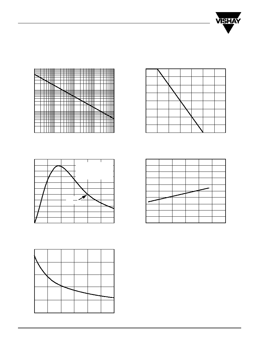
0
25
50
75
100
0
75
25
50
100
125
150
175
P
eak Pulse P
o
w
er (P
PP
) or Current (I
PP
)
Der
ating in P
ercentage
, %
T
A
-- Ambient Temperature (
∞
C)
Fig. 2 ≠ Pulse Derating Curve
P
PPM
--
P
eak Pulse P
o
w
er (kW)
Fig. 1 ≠ Non-Repetitive Peak Pulse Power
vs. Pulse Time
0.1
1
10
0.1
1.0
10
td -- Pulse Duration (
µ
s)
100
1000
0
50
100
90
80
70
60
40
30
20
10
110
I
PPM
--
P
eak Pulse Current, % I
RSM
Fig. 3 ≠ Pulse Waveform
Pulse Width (td)
is defined as the point
where the peak current
decays to 50% of I
PPM
0
10
5
15
20
30
25
t -- Time (
µ
s)
I
PP
--
Peak Pulse Current (A)
Fig. 4 ≠ Clamping Voltage
vs. Peak Pulse Current
0.01
t
d
= I
PP
2
0
10
20
18
16
14
12
8
6
4
2
V
C
--
Clamping V
oltage
(V)
0
10
5
15
20
25
30
100
200
300
250
150
350
C
J
--
J
unction Capacitance (pF)
Fig. 5 ≠ Typical Junction Capacitance
0
2
1
3
4
6
5
V
R
-- Reverse Voltage (V)