 | ÐлекÑÑоннÑй компоненÑ: RFW322-M | СкаÑаÑÑ:  PDF PDF  ZIP ZIP |
/home/web/chipfind.ru/datasheet/html/vishay/195050
Vishay RFWaves
RFW322-M
Document Number 81218
Rev. 1.0, 16-Nov-05
www.vishay.com
1
For more information please contact: RFTransceivers@vishay.com
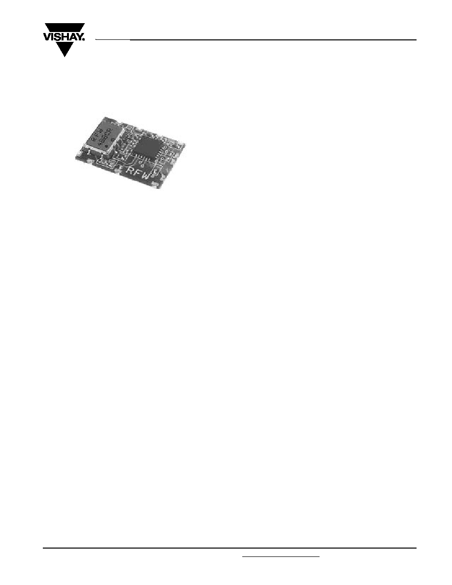
RFW322-M Transceiver Module
FEATURES
·
Designed for short range wireless communication
in the 2.4 GHz - world wide license free band
·
Data rate - up to 3 mbit/s
·
Simple 3 line digital interface
·
Low power consumption - ideal for battery operated
devices
·
+ 6 dBm typical peak output transmission power
·
- 73 dBm typical sensitivity
·
Complies with FCC regulations
·
Wide range operating voltage (2.6 - 3.5 V)
·
Unique Direct Sequence Spread Spectrum Code
·
Short signal acquisition time (1.2 µs)
The company's products are covered by one or more
of the following:
Taiwan Patent No. 155994, Taiwan Patent No.
176767, USA Patent No. 6,535,545. Other patents
pending
DESCRIPTION
The RFW322-M ISM Transceiver Module is a short-
range wireless radio transceiver, designed by Vishay
RFWaves*. The transceiver is intended for use in the
world wide unlicensed Industrial, Scientific and Medi-
cal (ISM) band of 2400 - 2483.5 MHz, complying with
worldwide regulations and standards.
The module core consists of 2 chips, offering small
size, low power consumption and simple integration
with applications.
The module antenna interface reflects a 200
differ-
ential impedance.
Module has 3 digital control lines. The data I/O line is
a serial interface. RFW322-M the transceiver was
designed for low power consumption. During standby,
the transceiver almost does not consume any power
(0.1 µA at Vcc = 3 V). It features a very short wakeup
time of 20 µs, and the signal acquisition time is only 1.2 µs.
Thus, by using the standby mode in a frequent man-
ner, an efficient power consumption management
method can be applied.
The communication link between the transceivers is
based on a unique Direct Sequence Spread Spectrum
(DSSS) pulse pipe. The modulation scheme is 100 %
Amplitude Shift Keying (ASK).
The module interface has 12 pads and is soldered on
a motherboard PCB like a regular SMT component.
* Vishay Advanced Technologies ltd. -
RFWaves division
www.vishay.com
2
Document Number 81218
Rev. 1.0, 16-Nov-05
Vishay RFWaves
RFW322-M
For more information please contact: RFTransceivers@vishay.com
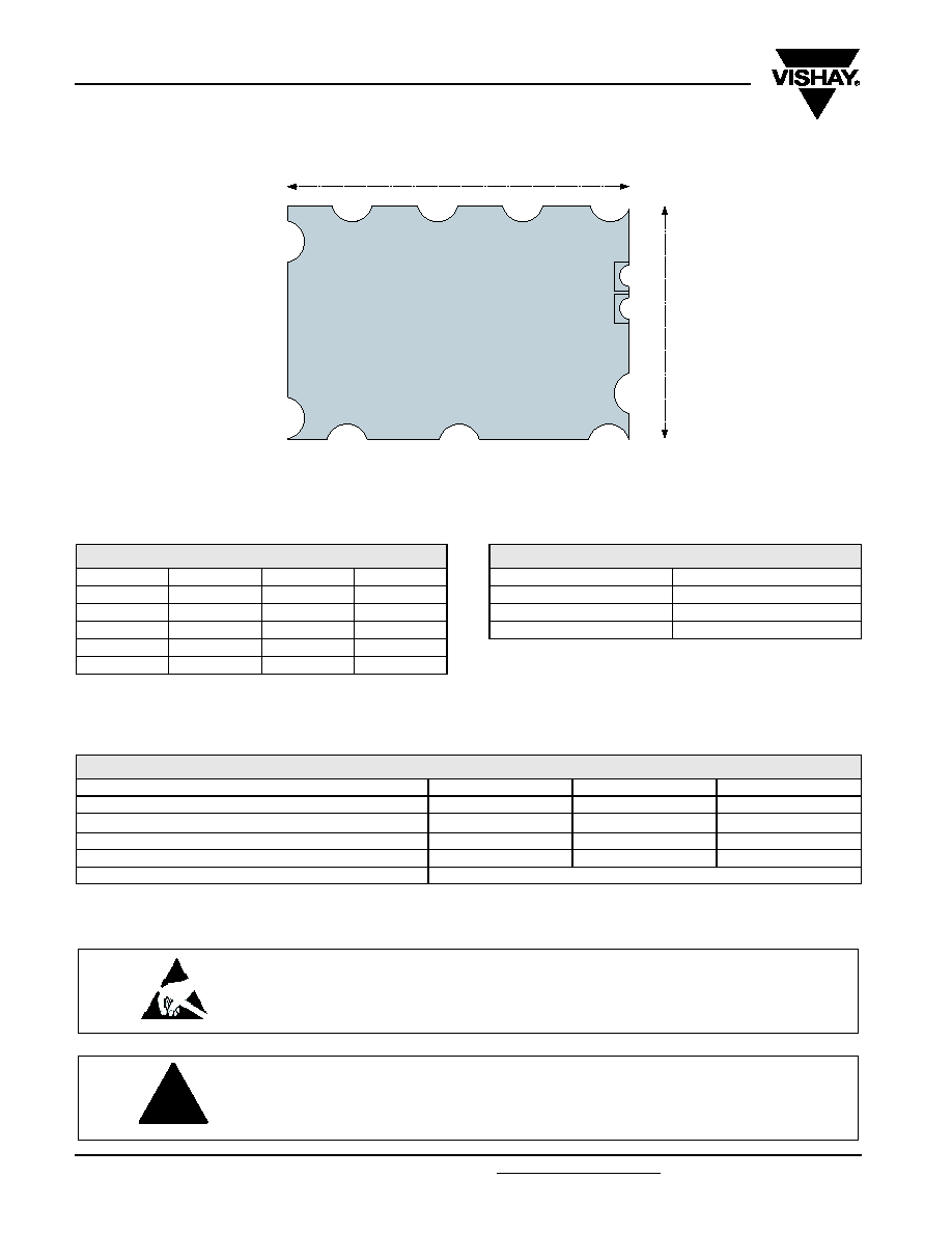
PIN OUT AND MECHANICAL DIMENSIONS in millimeters
Stresses exceeding those listed under "Absolute Maximum Rating" may cause permanent damage to the devices. These are stress ratings only,
and functional operation of the devices at these or any other conditions, beyond those indicated in the operational sections of the datasheet, is
not implied. Exposure to absolute maximum rating conditions for extended periods may affect devices reliability.
Top View
16.1
11
1
2
3
4
5
6
7
8
9
10
11
12
19579
PINOUT
1
VCC RF
7
TX/RX
2
ACT
8
TXD/RXD
3
VCC PD
9
VCC GD
4
GND
10
VCC OSC
5
GND
11
RF1
6
RSSI
12
RF2
MECHANICAL DIMENSIONS (mm)
Overall length
16.1
Overall width
11
PCB thickness
0.6
Max overall thickness
2.5
ABSOLUTE MAXIMUM RATING
PARAMETER
MIN
MAX
UNIT
Supply voltage
- 0.3
6.0
V
All input or output voltages with respect to ground
- 0.3
V
cc
+ 0.3
V
Temperature under bias
- 10
70
°C
Storage temperature
- 60
100
°C
Digital output short-circuit duration (to GND)
continues
These devices have limited built-in ESD protection. The leads should be shorted together
or the device placed in conductive foam during storage or handling to prevent electrostatic
damage to the I/O buffers.
Life Support Policy and Use in Safety-Critical Applications
Vishay RFWaves' products are not authorized for use in life-support or
saftey-critical applications.
!
Document Number 81218
Rev. 1.0, 16-Nov-05
www.vishay.com
3
Vishay RFWaves
RFW322-M
For more information please contact: RFTransceivers@vishay.com
* ESD protected pin.
TRANSCEIVER INTERFACE The RFW322-M transceiver includes the following 12 pads interface.
NAME
CHARACTERISTIC
V
CC
GD
Transmitter pulse generator power supply input. A regulated voltage of 2.6 - 3.5 Volts.
V
CC
RF
RF amplifier power supply input. A regulated voltage of 2.6 - 3.5 Volts.
V
CC
OSC
Oscillator power supply input. A regulated voltage of 2.6 - 3.5 Volts.
V
CC
PD
Receiver peak detector power supply input. A regulated voltage of 2.6 - 3.5 Volts.
GND
Apply the supply ground to this pin.
GND
Apply the supply ground to this pin.
Tx/Rx*
Mode selection input. Apply V
cc
for transmit mode.
Apply 0 V (GND) for receive mode.
ACT*
Apply 0 V (GND) for standby mode.
Apply V
cc
to this pin to turn the module on.
It typically takes the module 20 µs to wake up into a fully operational mode.
CMOS-level pin.
TxD/RxD*
In Tx mode this is an input pin, positive edge trigger. Every time TxD goes from GND to
V
cc
, a spread bit is transmitted.
In Rx mode this is an output pin.
CMOS-level pin.
RSSI
When used, reflects the average RF power detected by the receiver.
Connect to the RSSI port in the RFW-D100 or any equivalent interface.
RF1 / RF2
Connect a 200 ohm differential impedance antenna to this port, or a proper matching
circuit to any other antenna.
ELECTRICAL CHARACTERISTICS
T
A
= 25 °C, V
CC
= 2.7 V to 3.3 V, unless otherwise specified.
PARAMETER
TEST CONDITIONS
SYMBOL
MIN
TYP.
MAX
UNIT
Supply voltage (All 3 ports)
V
CC
2.6
3.3
3.5
V
Operating ambient temperature
T
a
0
+ 25
+ 50
°C
Current consumption in standby
mode
ACT = GND
I/O = High Z at V
cc
= 3 V
I
shdn
0.1
µA
Wakeup time
T
wa
20
µs
All input pins (TxD/RxD, ACT, Tx/Rx)
Rise time
T
r
8
1000
ns
Fall time
T
f
8
1000
ns
Input capacitance
C
in
10
PF
ACT
Logic high input
V
ih act
V
cc
- 0.8
V
cc
V
Logic low input
V
il act
GND
0.8
V
Sink current
ACT = V
cc
I
si_act
24
50
µA
Source current
ACT = GND
I
src_act
1
µA
Tx/Rx
Logic high input
V
ih tr
V
cc
- 0.8
V
cc
V
Logic low input
V
il tr
GND
0.8
V
Source current
I
src_tr
1
µA
Sink current
ACT = GND
I
si_shdn
1
µA
TxD/RxD
Source current in standby and
transmit mode
ACT = GND
I
src_shdn
1
µA
Sink current in standby and
transmit mode
ACT = GND
I
si_shdn
1
µA
Transmit to receive transition
time
T
t_to_r
2.5
µs
Receive to transmit transition
time
T
r_to_t
2.5
µs
Bit rate
3
Mb/s
www.vishay.com
4
Document Number 81218
Rev. 1.0, 16-Nov-05
Vishay RFWaves
RFW322-M
For more information please contact: RFTransceivers@vishay.com
(1)
When transmitting a uniform distribution of `1' and `0' bits. This assupmtion is not relevant in 3 Mbps!
(2)
Depends on test platform.
RECEIVER CHARACTERISTICS T
A
= 25 °C, V
CC
= 2.7 V to 3.3 V, unless otherwise specified.
PARAMETER
TEST CONDITIONS
SYMBOL
MIN
TYP.
MAX
UNIT
Signal acquisition time
T
acq
1.2
1.5
µs
Sensitivity
at BER = 10
-3
Sens
- 73
- 70
dBm
peak
RxD
Output voltage high
1 mA load sync current
RxDVH
V
cc
- 0.8
V
cc
V
Output voltage low
1 mA load source
current
RxDVL
0
0.8
V
Output capacitance
C
out
10
pF
Pulse length
T
pw
ns
Current consumption
RF power at antenna port
< - 40 dBm peak
Bit rate = 3 Mb/s
Is
34
mA
Emission level between 30 MHz
and 1 GHz
- 57
dBm
Emission level between 1 GHz and
12.75 GHz
- 47
dBm
RSSI
Allowed source current
I
src RS
50
nA
Allowed sink current
I
si_RS
50
nA
Allowed load capacitance
C
Io RS
20
pf
Output voltage
V_SAT
0.4
1.2
V
Voltage to received power slope
V to P
6
mV / dB
TRANSMITTER CHARACTERISTICS T = 25 °C, V
CC
= 2.7 V to 3.3 V, unless otherwise specified.
PARAMETER
TEST CONDITIONS
SYMBOL
MIN
TYP.
MAX
UNIT
Transmit power peak
Pout
max
2
6
dBm
TxD
Logic high input
V
ih d
V
cc
- 0.8
V
cc
V
Logic low input
V
il d
GND
0.8
V
Source current
I
src_di
1
µA
Sink current
I
si_di
1
µA
Pulse length
T
dil
20
Not limited
ns
Current consumption
Bit rate = 3 Mb/s
(1)
Is
34
mA
Current consumption - No data
transmitted
TxD/RxD = 0
Isnd
7
mA
Bandwidth
at - 10 dBc
BW
30
MHz
Out of band spurious
(> 1 GHz)
(2)
at RBW = 1 MHz;
at VBW = 1 MHz
Spur
- 20
dBm
Time from data into output
power
T
d
400
450
500
ns
Central frequency
Cf
2.439
2.440
2.441
GHz
Document Number 81218
Rev. 1.0, 16-Nov-05
www.vishay.com
5
Vishay RFWaves
RFW322-M
For more information please contact: RFTransceivers@vishay.com
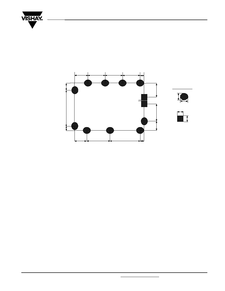
FOOTPRINT
The following diagram shows the physical footprint of
the RFW322-M module, which should be implement-
ed.
***Note: The pcb area under the module (CS layer
only) must be considered as void and not include any
conducting metal.
**All figures are in mm units. Measurements are taken from the middle of the solder pads.
NOTICE
Specifications of the products displayed herein are
subject to change without notice. Vishay Intertechnol-
ogy, Inc., or anyone one its behalf, assumes no
responsibility or liability for any errors or inaccuracies.
Information contained herein is intended to provide a
product description only. No license, express or
implied, by estoppel or otherwise, to any intellectual
property rights is granted by this document. Except as
provided in Vishay's terms and conditions of sale for
such products, Vishay assumes no liability whatso-
ever, and disclaims any express or implied warranty,
relating to sale and/or use of Vishay products including
liability or warranties relating to fitness for a particular
purpose, merchantability, or infringement of any
patent, copyright, or other intellectual property right.
The products shown herein are not designed for use in
medical, life-saving, or life-sustaining applications.
Customers using or selling these products for use in
such applications do so at their own risk and agree to
fully indemnify Vishay for any damages resulting from
such improper use or sale.
Footprint
3.3
2
1
4
3
9
7
8
12
11
4
3.1
4
4.1
0.9
4
10
2.2
7
5.4
2.8
8.3
1.6
0.2
1.3
1.3
1.7
1.4
0.9
1.1
Pad Dimensions
6
5
19580
Document Outline