
SAC5.0 thru SAC50 Series
Vishay Semiconductors
formerly General Semiconductor
Document Number 88379
www.vishay.com
03-May-02
1
Low Capacitance T
RANS
Z
ORB
Æ
Transient Voltage Suppressors
Peak Pulse Power 500W
Stand-off Voltage 5.0 to 50V
0.034 (0.86)
0.028 (0.71)
Dia.
0.140 (3.6)
0.104 (2.6)
Dia.
0.230 (5.8)
0.300 (7.6)
1.0 (25.4)
min.
1.0 (25.4)
min.
DO-204AC (DO-15)
Maximum Ratings and Thermal Characteristics
(T
A
= 25∞C unless otherwise noted)
Parameter
Symbol
Limit
Unit
Peak pulse power dissipation with a 10/1000
µ
s waveform
P
PPM
Minimum 500
(1)
W
Steady state power dissipation at T
L
= 75
∞
C with
P
M(AV)
3.0
W
lead lengths or 0.375" (9.5mm)
Peak pulse power surge current with a
I
PPM
See Next Table
(1)
A
10/1000
µ
s waveform (Fig. 3)
Operating junction and storage temperature range
T
J
, T
STG
≠55 to +175
∞
C
Note: (1) Non-repetitive current pulse, per Fig.3 and derated above T
A
= 25∞C per Fig. 2
Features
∑ Plastic package has Underwriters Laboratory
Flammability Classification 94V-0
∑ Glass passivated junction
∑ 500W peak pulse power capabililty with a
10/1000
µ
s waveform, repetition rate (duty cycle):
0.01%
∑ Excellent clamping capability
∑ Low incremental surge resistance
∑ Very fast response time
∑ Ideal for data line applications
∑ High temperature soldering guaranteed:
265
O
C/10 seconds, 0.375" (9.5mm) lead length,
5lbs. (2.3 kg) tension
Dimensions in inches and (millimeters)
Schematic
Diode
Transient
Voltage
Suppressor
Mechanical Data
Case: JEDEC DO-204AC molded plastic body over
passivated junction
Terminals: Solder plated axial leads, solderable per
MIL-STD-750, Method 2026
Polarity: Color band denotes TVS cathode
Mounting Position: Any
Weight: 0.015 oz., 0.4 g
Packaging Codes ≠ Options (Antistatic):
51 ≠ 1K per Bulk box, 10K/carton
54 ≠ 4K per 13" paper Reel
(52mm horiz. tape), 12K/carton
73 ≠ 2K per horiz. tape & Ammo box, 20K/carton

SAC5.0 thru SAC50 Series
Vishay Semiconductors
formerly General Semiconductor
www.vishay.com
Document Number 88379
2
03-May-02
Electrical Characteristics
Ratings at 25∞C ambient temperature unless otherwise specified.
Minimum
Maximum
Maximum
Maximum
Maximum
Working
Inverse
Peak
Breakdown
Reverse
Clamping
Peak Pulse
Junction
Inverse
Blocking
Inverse
Stand-off
Voltage
Leakage
Voltage
Current
Capacitance
Blocking
Leakage
Blocking
Voltage
(1)
at I
T
= 1.0mA
at V
WM
at I
PP
= 5.0A
per Fig. 3
at
Voltage
Current
Voltage
Part
V
WM
V
(BR)
I
D
V
C
I
PP
0 Volts
V
WIB
V
WIB
V
PIB
Number
(V)
(V)
(
µ
A)
(V)
(A)
(pF)
(V)
I
IB
(mA)
(V)
SAC5.0
5.0
7.60
300
10.0
44
50
75
1.0
100
SAC6.0
6.0
7.90
300
11.2
41
50
75
1.0
100
SAC7.0
7.0
8.33
300
12.6
38
50
75
1.0
100
SAC8.0
8.0
8.89
100
13.4
36
50
75
1.0
100
SAC8.5
8.5
9.44
50
14.0
34
50
75
1.0
100
SAC10
10
11.10
5.0
16.3
29
50
75
1.0
100
SAC12
12
13.30
5.0
19.0
25
50
75
1.0
100
SAC15
15
16.70
5.0
23.6
20
50
75
1.0
100
SAC18
18
20.00
5.0
28.8
15
50
75
1.0
100
SAC22
22
24.40
5.0
35.4
14
50
75
1.0
100
SAC26
26
28.90
5.0
42.3
11.1
50
75
1.0
100
SAC30
30
33.30
5.0
48.6
10.0
50
75
1.0
100
SAC36
36
40.00
5.0
60.0
8.6
50
75
1.0
100
SAC45
45
50.00
5.0
77.0
6.8
50
150
1.0
200
SAC50
50
55.50
5.0
88.0
5.8
50
150
1.0
200
Notes: (1) Non-repetitive current pulse, per Fig.3 and derated above T
A
= 25∞C per Fig. 2
SAC5.0 thru SAC50 Series
Vishay Semiconductors
formerly General Semiconductor
Document Number 88379
www.vishay.com
03-May-02
3
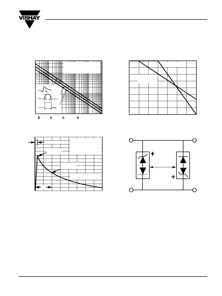
Ratings and
Characteristic Curves
(T
A
= 25∞C unless otherwise noted)
0
50
100
150
175
0
25
50
75
100
Average Power
Peak Power
(single pulse)
Low Capacitance
TVS
Fig. 2 - Power Derating Curve
Fig. 4 - AC Line Protection Application
Percentage of Rated Power (%)
T
L
Lead Temperature (
∞
C)
Application Note: Device must be used
with two units in parallel, opposite in polarity
as shown in circuit for AC signal line
protection.
0
50
100
150
I
PPM
≠
P
eak Pulse Current, % I
RSM
Fig. 3 ≠ Pulse Waveform
T
J
= 25
∞
C
Pulse Width (td)
is defined as the point
where the peak current
decays to 50% of I
PPM
tr = 10
µ
sec.
Peak Value
I
PPM
Half Value ≠ IPP
I
PPM
2
td
10/1000
µ
sec. Waveform
as defined by R.E.A.
0
1.0
2.0
3.0
4.0
t ≠ Time (ms)
0.1 s
1.0
s
10
s
100
s
1.0ms
10ms
0.1
1.0
10
30
Fig. 1 ≠ Peak Pulse Power Rating Curve
P
PPM
≠
P
eak Pulse P
o
w
er (kW)
Non-repetitive Pulse
Waveform shown in Fig. 3
T
A
= 25
∞
C
td ≠ Pulse Width (sec.)
t
d
t
d
t
d
Current Waveforms
Impulse
Exponential
Decay
Half Sine
Square
P
PK
".5"
P
PK
P
PK
t
d
= 7 tp