 | –≠–ª–µ–∫—Ç—Ä–æ–Ω–Ω—ã–π –∫–æ–º–ø–æ–Ω–µ–Ω—Ç: SI1901DL | –°–∫–∞—á–∞—Ç—å:  PDF PDF  ZIP ZIP |

Si1901DL
Vishay Siliconix
New Product
Document Number: 71304
S-01886--Rev. A, 28-Aug-00
www.vishay.com
1
P-Channel 20-V (D-S) MOSFET
PRODUCT SUMMARY
V
DS
(V)
r
DS(on)
(
W
)
I
D
(mA)
≠20
3.8 @ V
GS
= ≠4.5 V
≠180
≠20
5.0 @ V
GS
= ≠2.5 V
≠100
Marking Code
QD
XX
Lot Traceability
and Date Code
Part # Code
YY
SOT-363
SC-70 (6-Leads)
S
1
1
3
G
1
2
D
2
6
4
5
D
1
G
2
S
2
Top View
ABSOLUTE MAXIMUM RATINGS (T
A
= 25_C UNLESS OTHERWISE NOTED)
Parameter
Symbol
Limit
Unit
Drain-Source Voltage
V
DS
≠20
V
Gate-Source Voltage
V
GS
"
8
V
Continuous Drain Current
(T
J
= 150
_
C)
a
T
A
= 25
_
C
I
D
≠180
A
Continuous Drain Current
(T
J
= 150 C)
a
T
A
= 70
_
C
I
D
≠140
mA
Pulsed Drain Current
I
DM
≠500
Maximum Power Dissipation
a
T
A
= 25
_
C
P
D
0.20
W
Maximum Power Dissipation
a
T
A
= 70
_
C
P
D
0.13
W
Operating Junction and Storage Temperature Range
T
J
, T
stg
≠55 to 150
_
C
THERMAL RESISTANCE RATINGS
Parameter
Symbol
Limit
Unit
Maximum Junction-to-Ambient
a
R
thJA
625
_
C/W
Notes
a.
Surface Mounted on FR4 Board, t
v
10 sec.
Si1901DL
Vishay Siliconix
New Product
www.vishay.com
2
Document Number: 71304
S-01886--Rev. A, 28-Aug-00
SPECIFICATIONS (T
J
= 25_C UNLESS OTHERWISE NOTED)
Parameter
Symbol
Test Condition
Min
Typ
Max
Unit
Static
Drain-Source Breakdown Voltage
V
(BR)DSS
V
DS
= 0 V, I
D
= ≠10
m
A
≠20
≠24
V
Gate-Threshold Voltage
V
GS(th)
V
DS
= V
GS
, I
D
= ≠50
m
A
≠0.4
≠0.9
≠1.5
V
Gate-Body Leakage
I
GSS
V
DS
= 0 V, V
GS
=
"
8 V
"
2
"
100
nA
Zero Gate Voltage Drain Current
I
DSS
V
DS
= ≠20 V, V
GS
= 0 V
≠0.001
≠100
nA
Zero Gate Voltage Drain Current
I
DSS
V
DS
= ≠20 V, V
GS
= 0 V, T
J
= 55
_
C
≠1
m
A
On-State Drain Current
a
I
D(on)
V
GS
v
≠4.5 V, V
DS
= ≠8.0 V
≠400
mA
On-State Drain Current
a
I
D(on)
V
GS
v
≠2.5 V, V
DS
= ≠5.0 V
≠120
mA
Drain Source On State Resistance
a
r
DS(
)
V
GS
= ≠4.5 V, I
D
= ≠180 mA
2.6
3.8
W
Drain-Source On-State Resistance
a
r
DS(on)
V
GS
= ≠2.5 V, I
D
=
≠
75 mA
4.0
5.0
W
Forward Transconductance
a
g
fs
V
DS
= ≠2.5 V, I
D
= ≠50 mA
200
mS
Diode Forward Voltage
a
V
SD
I
S
= ≠50 mA, V
GS
= 0 V
≠0.7
≠1.2
V
Dynamic
Total Gate Charge
Q
g
V
5 0 V V
4 5 V I
100
A
350
450
C
Gate-Source Charge
Q
gs
V
DS
= ≠5.0 V,
V
GS
= ≠4.5 V, I
D
= ≠100 mA
25
pC
Gate-Drain Charge
Q
gd
125
Input Capacitance
C
iss
V
5 0 V V
0 V f
1 MH
20
F
Output Capacitance
C
oss
V
DS
= ≠5.0 V,
V
GS
= 0 V, f = 1 MHz
14
pF
Reverse Transfer Capacitance
C
rss
5
Switching
b, c
Turn-On Delay Time
t
d(on)
V
3 0 V R
100
W
7
12
Rise Time
t
r
V
DD
= ≠3.0 V, R
L
= 100
W
I
0 25 A V
4 5 V R
10
W
25
35
ns
Turn-Off Delay Time
t
d(off)
DD
,
L
I
D
= ≠0.25 A, V
GEN
= ≠4.5 V, R
G
= 10
W
19
30
ns
Fall Time
t
f
9
15
Notes
a.
Pulse test; pulse width
v
300
m
s, duty cycle
v
2%.
b.
For design only, not subject to production testing.
c.
Switching time is essentially independent of operating temperature.

Si1901DL
Vishay Siliconix
New Product
Document Number: 71304
S-01886--Rev. A, 28-Aug-00
www.vishay.com
3
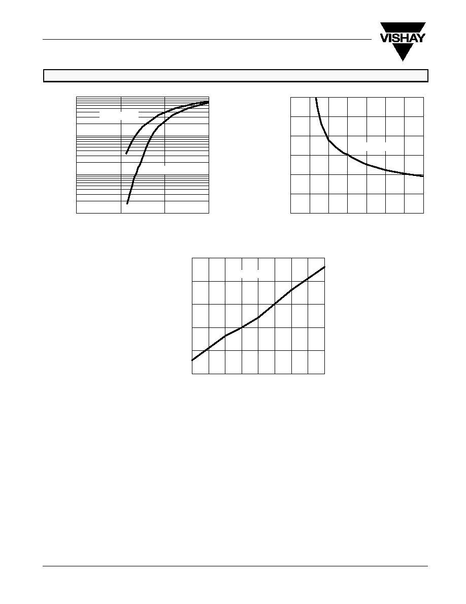
TYPICAL CHARACTERISTICS (25_C UNLESS NOTED)
0
0.1
0.2
0.3
0.4
0.5
0
0.5
1.0
1.5
2.0
2.5
3.0
0
2
4
6
8
0
0.5
1.0
1.5
2.0
2.5
3.0
0
0.2
0.4
0.6
0.8
1.0
1.2
0
1
2
3
4
0
2
4
6
8
10
0
100
200
300
400
500
600
0.6
0.8
1.0
1.2
1.4
1.6
≠50
≠25
0
25
50
75
100
125
150
0
9
18
27
36
45
0
3
6
9
12
25
_
C
T
C
= ≠55
_
C
C
rss
C
oss
C
iss
V
DS
= 6 V
I
D
= 80 mA
V
GS
= 4.5 V
I
D
= 180 m A
V
GS
= 4.5 V
V
GS
= 2.5 V
2 V
125
_
C
2.5 V
Output Characteristics
Transfer Characteristics
Gate Charge
On-Resistance vs. Drain Current
V
DS
≠ Drain-to-Source Voltage (V)
≠ Drain Current (A)
I
D
V
GS
≠ Gate-to-Source Voltage (V)
≠ Drain Current (A)
I
D
≠ Gate-to-Source V
oltage
(V)
Q
g
≠ Total Gate Charge (pC)
V
DS
≠ Drain-to-Source Voltage (V)
C ≠ Capacitance (pF)
V
GS
≠ On-Resistance (
r
DS(on)
W
)
I
D
≠ Drain Current (A)
Capacitance
On-Resistance vs. Junction Temperature
T
J
≠ Junction Temperature (
_
C)
(Normalized)
≠ On-Resistance (
r
DS(on)
W
)
3 V
3.5 V
4 V
5 V
4.5 V
Si1901DL
Vishay Siliconix
New Product
www.vishay.com
4
Document Number: 71304
S-01886--Rev. A, 28-Aug-00
TYPICAL CHARACTERISTICS (25_C UNLESS NOTED)
≠0.2
≠0.1
0.0
0.1
0.2
0.3
≠50
≠25
0
25
50
75
100
125
150
I
D
= 50
m
A
1.5
0
1
2
3
4
5
6
1
1.5
2.0
2.5
3.0
3.5
4.0
4.5
0.001
1
I
D
= 180 mA
0.00
0.5
01
T
J
= 150
_
C
Threshold Voltage
V
ariance (V)
V
GS(th)
T
J
≠ Temperature (
_
C)
Source-Drain Diode Forward Voltage
On-Resistance vs. Gate-to-Source Voltage
≠ On-Resistance (
r
DS(on)
W
)
V
SD
≠ Source-to-Drain Voltage (V)
V
GS
≠ Gate-to-Source Voltage (V)
≠ Source Current (A)
I
S
0.1
0.01
T
J
= 25
_
C