SMAJ5.0 thru 188CA
Vishay Semiconductors
formerly General Semiconductor
Document Number 88390
www.vishay.com
03-May-02
1
Surface Mount T
RANS
Z
ORB
ģ
Transient Voltage Suppressors
Stand-off Voltage 5.0 to 188V
Peak Pulse Power 400W
Devices for Bidirectional Applications
For bi-directional devices, use suffix C or CA (e.g. SMAJ10C, SMAJ10CA). Electrical characteristics apply in both directions.
Maximum Ratings & Thermal Characteristics
Ratings at 25įC ambient temperature unless otherwise specified.
Parameter
Symbol
Value
Unit
Peak pulse power dissipation with
P
PPM
400
W
a 10/1000
Ķ
s waveform
(1,2)
(see fig. 1)
Peak pulse current with a waveform
(1)
I
PPM
See Next Table
A
Peak forward surge current 8.3ms single half sine-wave
I
FSM
40
A
uni-directional only
(2)
Typical thermal resistance, junction to ambient
(3)
R
JA
120
į
C/W
Typical thermal resistance, junction to lead
R
JL
30
į
C/W
Operating junction and storage temperature range
T
J
, T
STG
≠55 to +150
į
C
Notes: (1) Non-repetitive current pulse, per Fig. 3 and derated above T
A
= 25įC per Fig. 2. Rating is 300W above 78V
(2) Mounted on 0.2 x 0.2" (5.0 x 5.0mm) copper pads to each terminal
(3) Mounted on minimum recommended pad layout
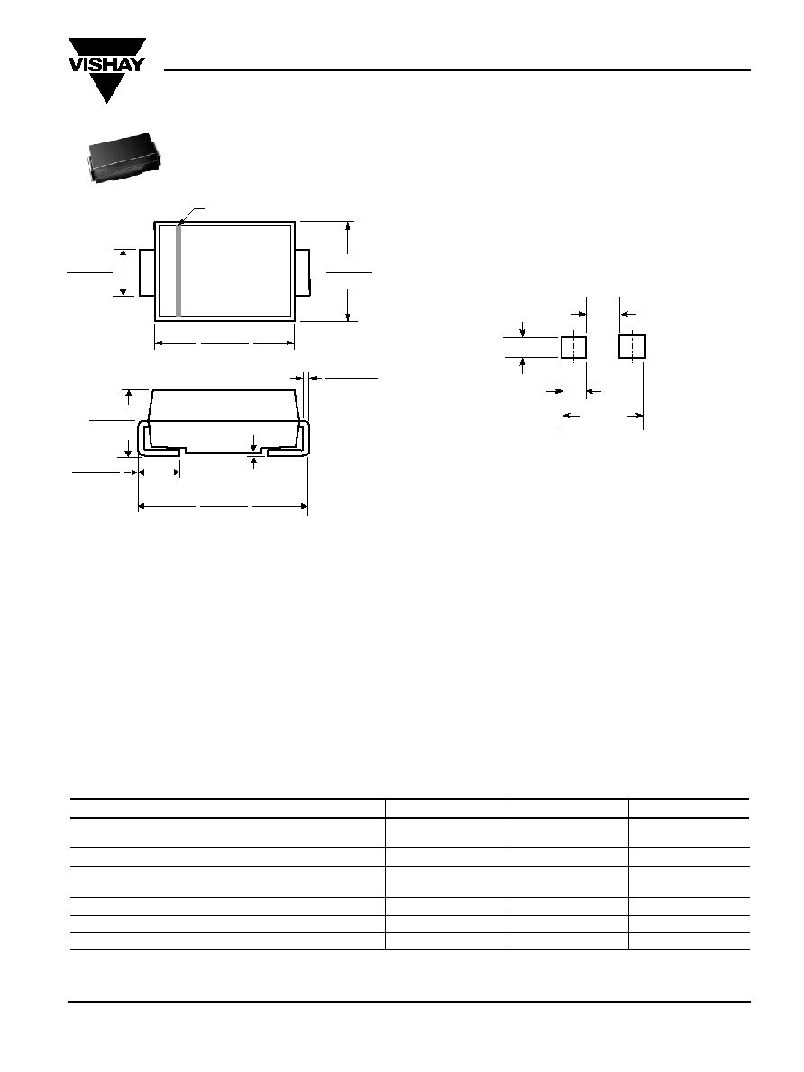
0.157 (3.99)
0.177 (4.50)
0.006 (0.152)
0.012 (0.305)
0.030 (0.76)
0.060 (1.52)
0.008 (0.203) MAX.
0.194 (4.93)
0.208 (5.28)
0.100 (2.54)
0.110 (2.79)
0.078 (1.98)
0.090 (2.29)
0.049 (1.25)
0.065 (1.65)
Cathode Band
Dimensions in inches
and (millimeters)
DO-214AC (SMA)
Features
∑ Plastic package has Underwriters Laboratory
Flammability Classification 94V-0
∑ Optimized for LAN protection applications
∑ Ideal for ESD protection of data lines in
accordance with IEC 1000-4-2 (IEC801-2)
∑ Ideal for EFT protection of data lines in
accordance with IEC 1000-4-4 (IEC801-4)
∑ Low profile package with built-in strain relief for
surface mounted applications
∑ Glass passivated junction
∑ Low incremental surge resistance, excellent clamping
capability
∑ 400W peak pulse power capability with a 10/1000
Ķ
s
waveform, repetition rate (duty cycle): 0.01% (300W
above 78V)
∑ Very fast response time
∑ High temperature soldering guaranteed:
250
į
C/10 seconds at terminals
Mechanical Data
Case: JEDEC DO-214AC molded plastic over
passivated chip
Terminals: Solder plated, solderable per MIL-STD-750,
Method 2026
Polarity: For uni-directional types the band denotes the
cathode, which is positive with respect to the anode
under normal TVS operation
Mounting Position: Any Weight: 0.002 oz., 0.064 g
Packaging Codes ≠ Options (Antistatic):
51 ≠ 1K per Bulk box, 20K/carton
61 ≠ 1.8K per 7" plastic Reel (12mm tape), 36K/carton
5A ≠ 7.5K per 13" plastic Reel (12mm tape), 75K/carton
0.094 MAX.
(2.38 MAX.)
0.220
(5.58) REF
0.066 MIN.
(1.68 MIN.)
0.052 MIN.
(1.32 MIN.)
Mounting Pad Layout
Extended
Voltage Range
SMAJ5.0 thru 188CA
Vishay Semiconductors
formerly General Semiconductor
www.vishay.com
Document Number 88390
2
03-May-02
Electrical Characteristics
Ratings at 25įC ambient temperature unless otherwise specified. V
F
= 3.5V at I
F
= 25A (uni-directional only)
Device
Breakdown Voltage
Maximum
Maximum
Maximum
Device Type
Marking
V
(BR)
at I
T
(1)
Test
Stand-off
Reverse Leakage Peak Pulse Surge
Clamping
Code
(V)
Current
Voltage
at V
WM
Current I
PPM
Voltage at I
PPM
UNI
BI Min
Max
I
T
(mA)
V
WM
(V)
I
D
(
Ķ
A)
(3)
(A)
(2)
V
C
(V)
SMAJ5.0
AD
WD
6.40
7.82
10
5.0
800
41.7
9.6
SMAJ5.0A
(5)
AE
WE
6.40 7.07
10
5.0
800
43.5
9.2
SMAJ6.0
AF
WF
6.67
8.15
10
6.0
800
35.1
11.4
SMAJ6.0A
AG
WG
6.67 7.37
10
6.0
800
38.8
10.3
SMAJ6.5
AH
WH
7.22
8.82
10
6.5
500
32.5
12.3
SMAJ6.5A
AK
WK 7.22
7.98
10
6.5
500
35.7
11.2
SMAJ7.0
AL
WL
7.78
9.51
10
7.0
200
30.1
13.3
SMAJ7.0A
AM
WM
7.78 8.60
10
7.0
200
33.3
12.0
SMAJ7.5
AN
WN
8.33
10.2
1.0
7.5
100
28.0
14.3
SMAJ7.5A
AP
WP
8.33 9.21
1.0
7.5
100
31.0
12.9
SMAJ8.0
AQ
WQ
8.89
10.9
1.0
8.0
50
26.7
15.0
SMAJ8.0A
AR
WR
8.89 9.83
1.0
8.0
50
29.4
13.6
SMAJ8.5
AS
WS
9.44
11.5
1.0
8.5
10
25.2
15.9
SMAJ8.5A
AT
WT
9.44 10.4
1.0
8.5
10
27.8
14.4
SMAJ9.0
AU
WU
10.0
12.2
1.0
9.0
5.0
23.7
16.9
SMAJ9.0A
AV
WV
10.0 11.1
1.0
9.0
5.0
26.0
15.4
SMAJ10
AW
WW
11.1
13.6
1.0
10
1.0
21.3
18.8
SMAJ10A
AX
WX
11.1 12.3
1.0
10
1.0
23.5
17.0
SMAJ11
AY
WY
12.2
14.9
1.0
11
1.0
19.9
20.1
SMAJ11A
AZ
WZ
12.2 13.5
1.0
11
1.0
22.0
18.2
SMAJ12
BD
XD
13.3
16.3
1.0
12
1.0
18.2
22.0
SMAJ12A
BE
XE
13.3 14.7
1.0
12
1.0
20.1
19.9
SMAJ13
BF
XF
14.4
17.6
1.0
13
1.0
16.8
23.8
SMAJ13A
BG
XG
14.4 15.9
1.0
13
1.0
18.6
21.5
SMAJ14
BH
XH
15.6
19.1
1.0
14
1.0
15.5
25.8
SMAJ14A
BK
XK
15.6 17.2
1.0
14
1.0
17.2
23.2
SMAJ15
BL
XL
16.7
20.4
1.0
15
1.0
14.9
26.9
SMAJ15A
BM
XM
16.7 18.5
1.0
15
1.0
16.4
24.4
SMAJ16
BN
XN
17.8
21.8
1.0
16
1.0
13.9
28.8
SMAJ16A
BP
XP
17.8 19.7
1.0
16
1.0
15.4
26.0
SMAJ17
BQ
XQ
18.9
23.1
1.0
17
1.0
13.1
30.5
SMAJ17A
BR
XR
18.9 20.9
1.0
17
1.0
14.5
27.6
SMAJ18
BS
XS
20.0
24.4
1.0
18
1.0
12.4
32.2
SMAJ18A
BT
XT
20.0 22.1
1.0
18
1.0
13.7
29.2
SMAJ20
BU
XU
22.2
27.1
1.0
20
1.0
11.2
35.8
SMAJ20A
BV
XV
22.2 24.5
1.0
20
1.0
12.3
32.4
SMAJ22
BW
XW
24.4
29.8
1.0
22
1.0
10.2
39.4
SMAJ22A
BX
XX
24.4 26.9
1.0
22
1.0
11.3
35.5
SMAJ24
BY
XY
26.7
32.6
1.0
24
1.0
9.3
43.0
SMAJ24A
BZ
XZ
26.7 29.5
1.0
24
1.0
10.3
38.9
SMAJ26
CD
YD
28.9
35.3
1.0
26
1.0
8.6
46.6
SMAJ26A
CE
YE
28.9 31.9
1.0
26
1.0
9.5
42.1
SMAJ28
CF
YF
31.1
38.0
1.0
28
1.0
8.0
50.0
SMAJ28A
CG
YG
31.1 34.4
1.0
28
1.0
8.8
45.4
SMAJ30
CH
YH
33.3
40.7
1.0
30
1.0
7.5
53.5
SMAJ30A
CK
YK
33.3 36.8
1.0
30
1.0
8.3
48.4
Notes: (1) Pulse test: t
p
50ms
(2) Surge current waveform per Fig. 3 and derate per Fig. 2
(3) For bi-directional types having V
WM
of 10 Volts and less, the I
D
limit is doubled
(4) All terms and symbols are consistent with ANSI/IEEE C62.35
(5) For the bidirectional SMAJ5.0CA, the maximum V
(BR)
is 7.25V.

SMAJ5.0 thru 188CA
Vishay Semiconductors
formerly General Semiconductor
Document Number 88390
www.vishay.com
03-May-02
3
Electrical Characteristics
Ratings at 25įC ambient temperature unless otherwise specified. V
F
= 3.5V at I
F
= 25A (uni-directional only)
Device
Breakdown Voltage
Maximum
Maximum
Maximum
Device Type
Marking
V
(BR)
at I
T
(1)
Test
Stand-off
Reverse Leakage Peak Pulse Surge
Clamping
Code
(V)
Current
Voltage
at V
WM
Current I
PPM
Voltage at I
PPM
UNI
BI Min
Max
I
T
(mA)
V
WM
(V)
I
D
(
Ķ
A)
(3)
(A)
(2)
V
C
(V)
SMAJ33
CL
YL
36.7
44.9
1.0
33
1.0
6.8
59.0
SMAJ33A
CM
YM
36.7 40.6
1.0
33
1.0
7.5
53.3
SMAJ36
CN
YN
40.0
48.9
1.0
36
1.0
6.2
64.3
SMAJ36A
CP
YP
40.0 44.2
1.0
36
1.0
6.9
58.1
SMAJ40
CQ
YQ
44.4
54.3
1.0
40
1.0
5.6
71.4
SMAJ40A
CR
YR
44.4 49.1
1.0
40
1.0
6.2
64.5
SMAJ43
CS
YS
47.8
58.4
1.0
43
1.0
5.2
76.7
SMAJ43A
CT
YT
47.8 52.8
1.0
43
1.0
5.8
69.4
SMAJ45
CU
YU
50.0
61.1
1.0
45
1.0
5.0
80.3
SMAJ45A
CV
YV
50.0 55.3
1.0
45
1.0
5.5
72.7
SMAJ48
CW
YW
53.3
65.1
1.0
48
1.0
4.7
85.5
SMAJ48A
CX
YX
53.3 58.9
1.0
48
1.0
5.2
77.4
SMAJ51
CY
YY
56.7
69.3
1.0
51
1.0
4.4
91.1
SMAJ51A
CZ
YZ
56.7 62.7
1.0
51
1.0
4.9
82.4
SMAJ54
RD
ZD
60.0
73.3
1.0
54
1.0
4.2
96.3
SMAJ54A
RE
ZE
60.0 66.3
1.0
54
1.0
4.6
87.1
SMAJ58
RF
ZF
64.4
78.7
1.0
58
1.0
3.9
103
SMAJ58A
RG
ZG
64.4 71.2
1.0
58
1.0
4.3
93.6
SMAJ60
RH
ZH
66.7
81.5
1.0
60
1.0
3.7
107
SMAJ60A
RK
ZK
66.7 73.7
1.0
60
1.0
4.1
96.8
SMAJ64
RL
ZL
71.1
86.9
1.0
64
1.0
3.5
114
SMAJ64A
RM
ZM
71.1 78.6
1.0
64
1.0
3.9
103
SMAJ70
RN
ZN
77.8
95.1
1.0
70
1.0
3.2
125
SMAJ70A
RP
ZP
77.8 86.0
1.0
70
1.0
3.5
113
SMAJ75
RQ
ZQ
83.3
102
1.0
75
1.0
3.0
134
SMAJ75A
RR
ZR
83.3 92.1
1.0
75
1.0
3.3
121
SMAJ78
RS
ZS
86.7
106
1.0
78
1.0
2.9
139
SMAJ78A
RT
ZT
86.7 95.8
1.0
78
1.0
3.2
126
SMAJ85
RU
ZU
94.4
115
1.0
85
1.0
2.0
151
SMAJ85A
RV
ZV
94.4 104
1.0
85
1.0
2.2
137
SMAJ90
RW
ZW
100
122
1.0
90
1.0
1.9
160
SMAJ90A
RX
ZX
100 111
1.0
90
1.0
2.1
146
SMAJ100
RY
ZY
111
136
1.0
100
1.0
1.7
179
SMAJ100A
RZ
ZZ
111 123
1.0
100
1.0
1.9
162
SMAJ110
VD
VD
122
149
1.0
110
1.0
1.5
196
SMAJ110A
SE
VE
122 135
1.0
110
1.0
1.7
177
SMAJ120
SF
VF
133
163
1.0
120
1.0
1.4
214
SMAJ120A
VG
VG
133 147
1.0
120
1.0
1.6
193
SMAJ130
SH
VH
144
176
1.0
130
1.0
1.3
231
SMAJ130A
VK
VK
144 159
1.0
130
1.0
1.4
209
SMAJ150
SL
VL
167
204
1.0
150
1.0
1.1
268
SMAJ150A
VM
VM
167 185
1.0
150
1.0
1.2
243
SMAJ160
SN
VN
178
218
1.0
160
1.0
1.0
287
SMAJ160A
SP
VP
178 197
1.0
160
1.0
1.2
259
SMAJ170
SQ
VQ
189
231
1.0
170
1.0
0.99
304
SMAJ170A
SR
VR
189 209
1.0
170
1.0
1.09
275
SMAJ188
ST
VT
209
255
1.0
188
1.0
0.9
344
SMAJ188A
SS
VS
209
231
1.0
188
1.0
0.91
328
Notes: (1) Pulse test: t
p
50ms
(2) Surge current waveform per Fig. 3 and derate per Fig. 2
(3) For bi-directional types having V
WM
of 10 Volts and less, the I
D
limit is doubled
(4) All terms and symbols are consistent with ANSI/IEEE C62.35
SMAJ5.0 thru 188CA
Vishay Semiconductors
formerly General Semiconductor
www.vishay.com
Document Number 88390
4
03-May-02
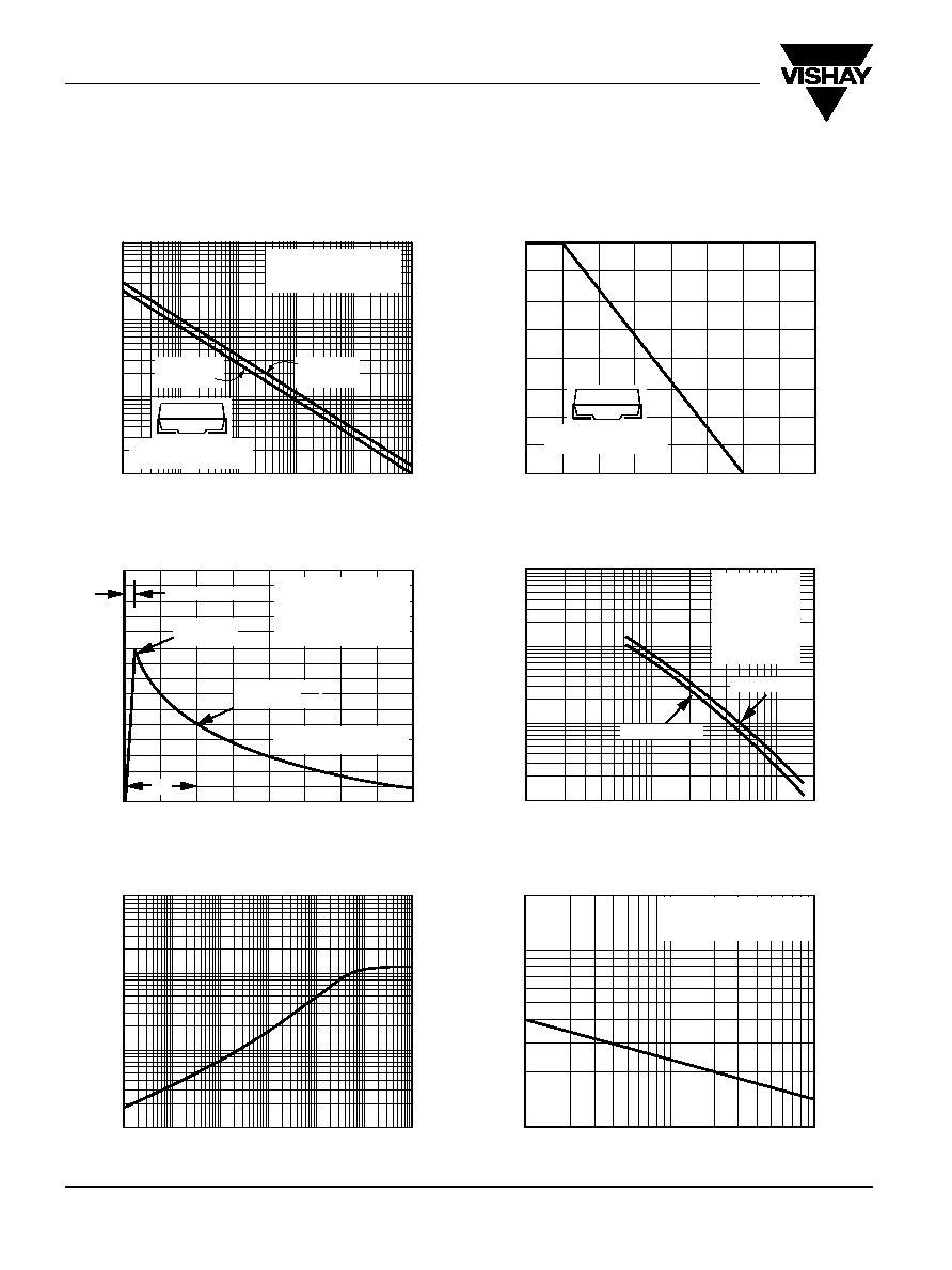
Ratings and
Characteristic Curves
(T
A
= 25įC unless otherwise noted)
0
25
50
75
100
0
75
25
50
100
125
150
175
200
Peak Pulse Power (P
PP
) or Current (I
PPM
)
Derating in Percentage, %
T
A
-- Ambient Temperature (
į
C)
1
5
10
50
100
t
p
-- Pulse Duration (sec)
Fig. 2 ≠ Pulse Derating Curve
P
PPM
--
Peak Pulse Power (kW)
Fig. 1 ≠ Peak Pulse Power Rating Curve
0.1
1
10
100
0.1
Ķ
s
1.0
Ķ
s
10
Ķ
s
t
d
-- Pulse Width (sec.)
100
Ķ
s
1.0ms
10ms
0.2 x 0.2" (5.0 x 5.0mm)
Copper Pad Areas
0.2 x 0.2" (5.0 x 5.0mm)
Copper Pad Areas
T
ransient
Thermal Impedance (
į
C/W)
Fig. 5 ≠ Typical Transient Thermal
Impedance
Non-repetitive Pulse
Waveform shown in Fig. 3
T
A
= 25
į
C
Fig. 6 - Maximum Non-Repetitive Forward
Surge Current Uni-Directional Only
I
FSM
--
Peak Forward Surge Current (A)
Number of Cycles at 60 Hz
C
J
--
Junction Capacitance (pF)
10
100
1,000
10,000
10
1
100
200
V
WM
-- Reverse Stand-off Voltage (V)
T
J
= 25
į
C
f = 1.0MHz
Vsig = 50mVp-p
Measured at
Stand-Off
Voltage, V
WM
Uni-Directional
Bi-Directional
10
50
100
200
T
J
= T
J
max.
8.3ms Single Half Sine-Wave
(JEDEC Method)
Fig. 4 ≠ Typical Junction Capacitance
1
10
100
1000
0.001
0.01
0.1
1
10
100
1000
0
50
100
150
I
PPM
--
Peak Pulse Current, % I
RSM
Fig. 3 ≠ Pulse Waveform
T
J
= 25
į
C
Pulse Width (td)
is defined as the point
where the peak current
decays to 50% of I
PPM
tr = 10
Ķ
sec.
Peak Value
I
PPM
Half Value -- IPP
I
PPM
2
td
10/1000
Ķ
sec. Waveform
as defined by R.E.A.
0
1.0
2.0
3.0
4.0
t -- Time (ms)
SMAJ5.0 --
SMAJ78
SMAJ85 --
SMAJ188