Document:1G5-0145
Rev.1
Page 1
VIS
VG4616321B/VG4616322B
262,144x32x2-Bit
Preliminary CMOS Synchronous Graphic RAM
Overview
The VG4616321(2) SGRAM is a high-speed CMOS synchronous graphics RAM containing 16M bits. It
is internally configured as a dual 256K x 32 DRAM with a synchronous interface (all signals are registered on
the positive edge of the clock signal, CLK). Each of the 256K x 32 bit banks is organized as 1024 rows by
256 columns by 32 bits. Read and write accesses to the SGRAM are burst oriented; accesses start at a
selected location and continue for a programmed number of locations in a programmed sequence. Accesses
begin with the registration of a BankActivate command which is then followed by a Read or Write command.
The VG4616321(2) provides for programmable Read or Write burst lengths of 1, 2, 4, 8, or full page,
with burst termination option. An Auto Precharge function may be enabled to provide a self-timed row pre-
charge that is initiated at the end of the burst sequence. The refresh functions, either Auto or Self Refresh
are easy to use. In addition, it features the write per bit and the masked block write functions.
By having a programmable Mode register and special mode register, the system can choose the best
suitable modes to maximize its performance. These devices are well suited for applications requiring high
memory bandwidth, and when combined with special graphics functions result in a device particularly well
suited to high performance graphics applications.
Features
∑ Fast access time from clock: 4.5/5/5.5ns
∑ Fast clock rate: 200/166/143 MHz
∑ Fully synchronous operation
∑ Internal pipelined architecture
∑ Dual internal banks(256K x 32-bit x 2-bank)
∑ Programmable Mode and Special Mode registers
- CAS Latency: 1, 2, or 3
- Burst Length: 1, 2, 4, 8, or full page
- Burst Type: interleaved or linear burst
- Burst Read Single Write
- Load Color or Mask register
∑ Burst stop function
∑ Individual byte controlled by DQM0-3
∑ Block write and write-per-bit capability
∑ Auto Refresh and Self Refresh
∑ 2048 refresh cycles/32ms
∑ Single + 3.3V power supply
∑ Input Reference Voltage : Vref = 1.5V 0.2V
∑ Interface: LVTTL and SSTL_3
∑ JEDEC 100-pin Plastic QFP package
0.3V
±
±

Document:1G5-0145
Rev.1
Page 2
VIS
VG4616321B/VG4616322B
262,144x32x2-Bit
Preliminary CMOS Synchronous Graphic RAM
Key Specifications
VG4616321/VG4616322
-5/6/7
t
CK
Clock Cycle time(min.)
5/6/7 ns
t
RAS
Row Active time(min.)
30/36/40 ns
t
AC
Access time from CLK(max.)
4.5/5/5.5 ns
t
RC
Row Cycle time(min.)
45/54/62 ns
DQ3
1
V
DDQ
2
DQ4
3
DQ5
4
V
SSQ
5
DQ6
6
DQ7
7
V
DDQ
8
DQ16
9
DQ17
10
11
DQ18
12
DQ19
13
V
DDQ
14
15
16
17
DQ21
18
19
V
SSQ
20
DQ23
21
22
DQM0
23
24
WE
25
CAS
26
RAS
27
CS
28
BS
29
A8
30
DQ28
V
DDQ
DQ27
DQ26
V
SSQ
V
DDQ
DQ15
DQ14
V
SSQ
DQ13
DQ12
V
DDQ
V
SS
DQ11
DQ10
DQ9
DQ8
NC/Vref
DQM3
DQM1
CLK
CKE
DSF
NC
A9
V
SSQ
V
DD
V
SS
DQ20
DQ22
V
DDQ
DQM2
80
79
78
77
76
75
74
73
72
71
70
69
68
67
66
65
64
63
62
61
60
59
58
57
56
55
54
53
52
51
DQ24
V
DD
V
SSQ
V
DDQ
D
Q
2
9
V
S
S
Q
D
Q
3
0
D
Q
3
1
V
S
S
N
C
N
C
N
C
N
C
N
C
N
C
N
C
N
C
N
C
D
Q
0
D
Q
1
D
Q
2
N
C
V
D
D
V
S
S
Q
8
2
8
3
8
4
8
5
8
6
8
7
8
8
8
9
9
0
9
1
9
2
9
3
9
4
9
5
9
6
9
7
9
8
9
9
1
0
0
8
1
A
7
A
6
A
5
A
4
V
S
S
N
C
N
C
N
C
N
C
N
C
N
C
N
C
N
C
N
C
A
3
A
2
A
0
N
C
V
D
D
A
1
4
9
4
8
4
7
4
6
4
5
4
4
4
3
4
2
4
1
4
0
3
9
3
8
3
7
3
6
3
5
3
4
3
3
3
2
3
1
5
0
Document:1G5-0145
Rev.1
Page 3
VIS
VG4616321B/VG4616322B
262,144x32x2-Bit
Preliminary CMOS Synchronous Graphic RAM
CS
RAS
CAS
WE
DSF
CLOCK
BUFFER
COMMAND
DECODER
COLUMN
COUNTER
ADDRESS
BUFFER
REFRESH
COUNTER
MODE
REGISTER
SPECIAL
MODE
REGISTER
CONTROL
SIGNAL
GENERATOR
COLOR
REGISTER
MASK
REGISTER
Column Decoder
1024 X 256 X 32
CELL ARRAY
(BANK #0)
R
o
w
D
e
c
o
d
e
r
Sense Amplifier
Sense Amplifier
1024 X 256 X 32
CELL ARRAY
(BANK #1)
R
o
w
D
e
c
o
d
e
r
Column Decoder
DQs
BUFFER
CLK
CKE
DQM0~3
DQ0
DQ31
|
A0
A8
~
BS
A9
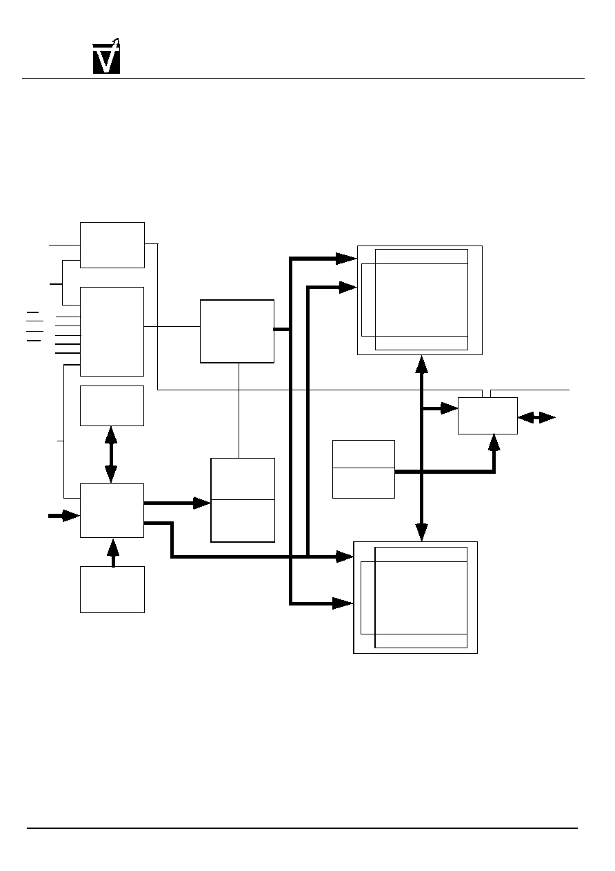
Block Diagram

Document:1G5-0145
Rev.1
Page 4
VIS
VG4616321B/VG4616322B
262,144x32x2-Bit
Preliminary CMOS Synchronous Graphic RAM
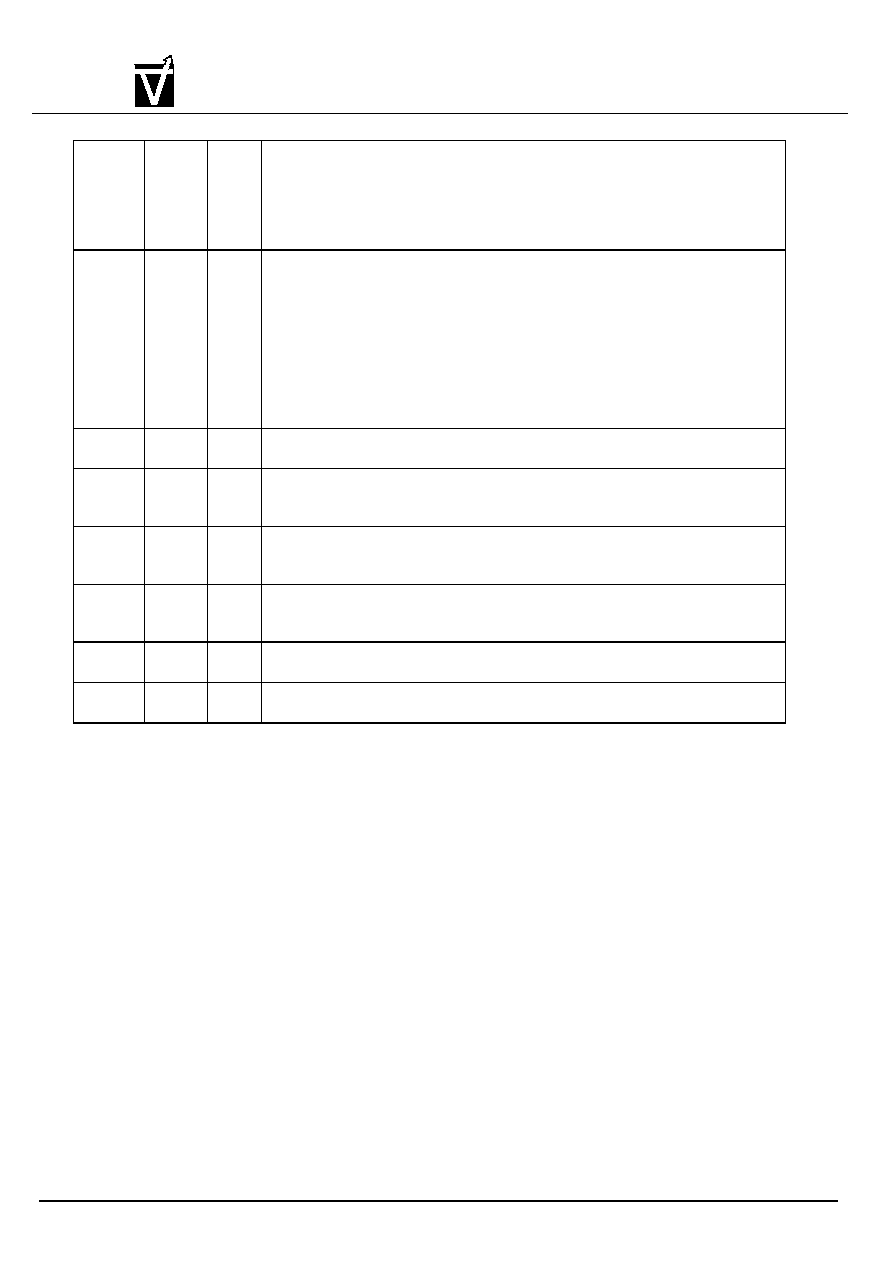
Table 1 shows the details for pin number, symbol, type, and description.
Table 1. Pin Description of VG4616321
Pin Num-
ber
Symbol Type Description
55
CLK
Input Clock: CLK is driven by the system clock. All SGRAM input signals are sampled on
the positive edge of CLK. CLK also increments the internal burst counter and con-
trol the output registers.
54
CKE
Input Clock Enable: CKE activates(HIGH) and deactivates(LOW) the CLK signal. If CKE
goes low synchronously with clock (set-up and hold time same as other inputs), the
internal clock is suspended from the next clock cycle and the state of output and
burst address is frozen as long as the CKE remains low. When both banks are in
the idle state, deactivating the clock controls the entry to the Power Down and Self
Refresh modes. CKE is synchronous except after the device enters Power Down
and Self Refresh modes, where CKE becomes asynchronous until after exiting the
same mode. The input buffers, including CLK, are disabled during Power Down
and Self Refresh modes providing low standby power.
29
BS
Input Bank Select: BS defines to which bank the BankActivate, Read, Write, or Bank-
Precharge command is being applied. BS is also used to program the 10th bit of
the Mode and Special Mode registers.
30-34,
47-51
A0-A9
Input Address Inputs: A0-A9 are sampled during the BankActivate command (row
address A0-A9) and Read/Write command (column address A0-A7 with A9 defin-
ing Auto Precharge) to select one location out of the 256K available in the respec-
tive bank. During a Precharge command, A9 is sampled to determine if both banks
are to be precharged (A9 = HIGH). The address inputs also provide the op-code
during a Mode Register Set or Special Mode Register Set command.
28
CS
Input Chip Select: CS enables (sampled LOW) and disables (sampled HIGH) the com-
mand decoder. All commands are masked when CS is sampled HIGH. CS provides
for external bank selection on systems with multiple banks. It is considered part of
the command code.
27
RAS
Input Row Address Strobe: The RAS signal defines the operation commands in con-
junction with the CAS and WE signals, and is latched at the positive edges of CLK.
When RAS and CS are asserted "LOW" and CAS is asserted "HIGH", either the
BankActivate command or the Precharge command is selected by the WE signal.
When the WE is asserted "HIGH" the BankActivate command is selected and the
bank designated by BS is turned on to the active state. When the WE is asserted
"LOW", the Precharge command is selected and the bank designated by BS is
switched to the idle state after precharge operation.
26
CAS
Input Column Address Strobe: The CAS signal defines the operation commands in
conjunction with the RAS and WE signals, and it is latched at the positive edges of
CLK. When RAS is held "HIGH" and CS is asserted "LOW", the column access is
started by asserting CAS "LOW". Then, the Read or Write command is selected by
asserting WE "LOW" or "HIGH".
25
WE
Input Write Enable: The WE signal defines the operation commands in conjunction with
the RAS and CAS signals, and it is latched at the positive edges of CLK. The WE
input is used to select the BankActivate or Precharge command and Read or Write
command.
53
DSF
Input Define Special Function: The DSF signal defines the operation commands in
conjunction with the RAS and CAS and WE signals, and it is latched at the positive
edges of CLK. The DSF input is used to select the masked write disable/enable
command and block write command, and the Special Mode Register Set cycle.
Document:1G5-0145
Rev.1
Page 5
VIS
VG4616321B/VG4616322B
262,144x32x2-Bit
Preliminary CMOS Synchronous Graphic RAM
23,56,24,
57
DQM0-
DQM3
Input Data Input/Output Mask: DQM0-DQM3 are byte specific, nonpersistent I/O buffer
controls. The I/O buffers are placed in a high-z state when DQM is sampled HIGH.
Input data is masked when DQM is sampled HIGH during a write cycle. Output data
is masked (two-clock latency) when DQM is sampled HIGH during a read cycle.
DQM3 masks DQ31-DQ24, DQM2 masks DQ23-DQ16, DQM1 masks DQ15-DQ8,
and DQM0 masks DQ7-DQ0.
97,98,100,
1,3,4,6,7,
60,61,63,
64,68,69,
71,72,9,
10,12,13,
17,18,20,
21,74,75,
77, 78,80,
81, 83, 84
DQ0-
DQ31
Input/
Output
Data I/O: The DQ0-31 input and output data are synchronized with the positive
edges of CLK. The I/Os are byte-maskable during Reads and Writes. The DQs also
serve as column/byte mask inputs during Block Writes.
30,36-45,
52,86-95
NC
-
No Connect: These pins should be left unconnected.
58
NC/Vref
-/Input No connect/Input Voltage Reference : It must be unconnected when the LVTTL
interface is used in the SGRAM. It must be applied to Vref (1.5V) when the SSTL-3
interface is used in the SGRAM.
2,8,14,22,
59,67,73,
79
V
DDQ
Supply DQ Power: Provide isolated power to DQs for improved noise immunity.
5,11,19,
62,70,76,
82,99
V
SSQ
Supply DQ Ground: Provide isolated ground to DQs for improved noise immunity.
15,35,65,
96
V
DD
Supply Power Supply: +3.3V
16,46,66,
85
V
SS
Supply Ground
0.3V
±