1
White Electronic Designs Corporation (508) 485-4000 www.whiteedc.com
June 2003 Rev. 1
ECO #16372
WED3DG6434V-D1
White Electronic Designs Corp reserves the right to change products or specifications without notice.
256MB- 32Mx64 SDRAM UNBUFFERED
n PC100 compatible
n Burst Mode Operation
n Auto and Self Refresh capability
n LVTTL compatible inputs and outputs
n Serial Presence Detect with EEPROM
n Fully synchronous: All signals are registered on the positive
edge of the system clock
n Programmable Burst Lengths: 1, 2, 4, 8 or Full Page
n 3.3 volt 6 0.3v Power Supply
n 144- Pin SO-DIMM JEDEC
The WED3DG6434V is a 32Mx64 synchronous DRAM module
which consists of sixteen 16Mx8 SDRAM components in sTSOP-
11 package, and one 2K EEPROM in an 8- pin TSSOP package
for Serial Presence Detect which are mounted on a 144 Pin SO-
DIMM multilayer FR4 Substrate.
DESCRIPTION
FEATURES
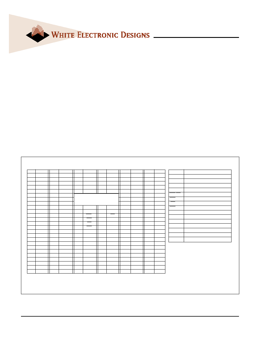
PIN CONFIGURATIONS (FRONT SIDE/BACK SIDE)
PIN NAMES
** These pins should be NC in the system which
does not support SPD.
Pin
Front
Pin
Back
Pin
Front
Pin
Back
Pin
Front
Pin
Back
1
VSS
2
VSS
51
DQ14
52
DQ46
95
DQ21
96
DQ53
3
DQ0
4
DQ32
53
DQ15
54
DQ47
97
DQ22
98
DQ54
5
DQ1
6
DQ33
55
VSS
56
VSS
99
DQ23
100
DQ55
7
DQ2
8
DQ34
57
NC
58
NC
101
VDD
102
VDD
9
DQ3
10
DQ35
59
NC
60
NC
103
A6
104
A7
11
VDD
12
VDD
105
A8
106
BA0
13
DQ4
14
DQ36
107
VSS
108
VSS
15
DQ5
16
DQ37
109
A9
110
BA1
17
DQ6
18
DQ38
61
CLK0
62
CKE0
111
A10/AP
112
A11
19
DQ7
20
DQ39
63
VDD
64
VDD
113
VDD
114
VDD
21
VSS
22
VSS
65
RAS
66
CAS
115
DQM2
116
DQM6
23
DQM0
24
DQM4
67
WE
68
CKE1
117
DQM3
118
DQM7
25
DQM1
26
DQM5
69
CS0
70
NC
119
VSS
120
VSS
27
VDD
28
VDD
71
CS1
72
NC
121
DQ24
122
DQ56
29
A0
30
A3
73
DNU
74
CLK1
123
DQ25
124
DQ57
31
A1
32
A4
75
VSS
76
VSS
125
DQ26
126
DQ58
33
A2
34
A5
77
NC
78
NC
127
DQ27
128
DQ59
35
VSS
36
VSS
79
NC
80
NC
129
VDD
130
VDD
37
DQ8
38
DQ40
81
VDD
82
VDD
131
DQ28
132
DQ60
39
DQ9
40
DQ41
83
DQ16
84
DQ48
133
DQ29
134
DQ61
41
DQ10
42
DQ42
85
DQ17
86
DQ49
135
DQ30
136
DQ62
43
DQ11
44
DQ43
87
DQ18
88
DQ50
137
DQ31
138
DQ63
45
VDD
46
VDD
89
DQ19
90
DQ51
139
VSS
140
VSS
47
DQ12
48
DQ44
91
VSS
92
VSS
141
**SDA
142
**SCL
49
DQ13
50
DQ45
93
DQ20
94
DQ52
143
VDD
144
VDD
VOLTAGE KEY
A0 A11
Address input (Multiplexed)
BA0-1
Select Bank
DQ0-63
Data Input/Output
CLK0,CLK1
Clock input
CKE0,CKE1
Clock Enable input
CS0,CS1
Chip select Input
RAS
Row Address Strobe
CAS
Column Address Strobe
WE
Write Enable
DQM0-7
DQM
VDD
Power Supply (3.3V)
VSS
Ground
SDA
Serial data I/O
SCL
Serial clock
DNU
Do not use
NC
No Connect
2
White Electronic Designs Corporation (508) 485-4000 www.whiteedc.com
June 2003 Rev. 1
ECO #16372
WED3DG6434V-D1
White Electronic Designs Corp reserves the right to change products or specifications without notice.
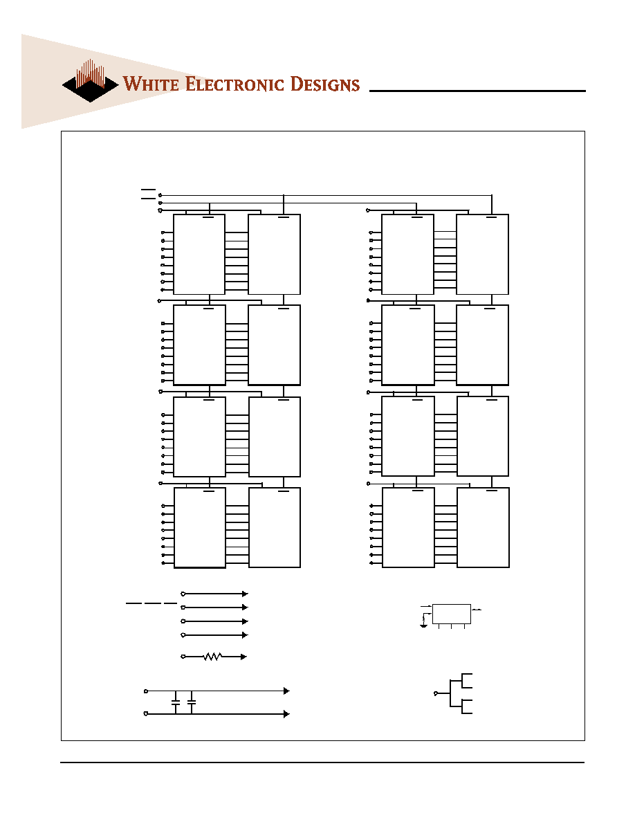
FUNCTIONAL BLOCK DIAGRAM
DQM0
DQ0
DQ1
DQ2
DQ3
DQ4
DQ5
DQ6
DQ7
U0
DQ0
DQ1
DQ2
DQ3
DQ4
DQ5
DQ6
DQ7
DQM CS
CS0
DQ0
DQ1
DQ2
DQ3
DQ4
DQ5
DQ6
DQ7
U4
DQ32
DQ33
DQ34
DQ35
DQ36
DQ37
DQ38
DQ39
DQM CS
DQM1
DQ0
DQ1
DQ2
DQ3
DQ4
DQ5
DQ6
DQ7
U1
DQ8
DQ9
DQ10
DQ11
DQ12
DQ13
DQ14
DQ15
DQM CS
DQ0
DQ1
DQ2
DQ3
DQ4
DQ5
DQ6
DQ7
U5
DQ40
DQ41
DQ42
DQ43
DQ44
DQ45
DQ46
DQ47
DQM CS
DQM5
DQM4
DQM2
DQ0
DQ1
DQ2
DQ3
DQ4
DQ5
DQ6
DQ7
U2
DQ16
DQ17
DQ18
DQ19
DQ20
DQ21
DQ22
DQ23
DQM CS
DQ0
DQ1
DQ2
DQ3
DQ4
DQ5
DQ6
DQ7
U6
DQ48
DQ49
DQ50
DQ51
DQ52
DQ53
DQ54
DQ55
DQM CS
DQM3
DQ0
DQ1
DQ2
DQ3
DQ4
DQ5
DQ6
DQ7
U3
DQ24
DQ25
DQ26
DQ27
DQ28
DQ29
DQ30
DQ31
DQM CS
DQ0
DQ1
DQ2
DQ3
DQ4
DQ5
DQ6
DQ7
U7
DQ56
DQ57
DQ58
DQ59
DQ60
DQ61
DQ62
DQ63
DQM CS
DQM7
DQM6
DQ0
DQ1
DQ2
DQ3
DQ4
DQ5
DQ6
DQ7
U8
DQM CS
DQ0
DQ1
DQ2
DQ3
DQ4
DQ5
DQ6
DQ7
U9
DQM CS
DQ0
DQ1
DQ2
DQ3
DQ4
DQ5
DQ6
DQ7
U10
DQM CS
DQ0
DQ1
DQ2
DQ3
DQ4
DQ5
DQ6
DQ7
U11
DQM CS
DQ0
DQ1
DQ2
DQ3
DQ4
DQ5
DQ6
DQ7
U12
DQM CS
DQ0
DQ1
DQ2
DQ3
DQ4
DQ5
DQ6
DQ7
U13
DQM CS
DQ0
DQ1
DQ2
DQ3
DQ4
DQ5
DQ6
DQ7
U14
DQM CS
DQ0
DQ1
DQ2
DQ3
DQ4
DQ5
DQ6
DQ7
U15
DQM CS
CS1
∑
∑
∑
∑
∑
∑
∑
∑
∑
∑
A0 ~ A11, BA0 & 1
CKE0
RAS, CAS, WE
SDRAM U0 ~ U15
SDRAM U0 ~ U15
SDRAM U0 ~ U7
10
DQn
Every DQpin of SDRAM
CKE1
SDRAM U8 ~ U15
V
D D
Vss
Two 0.1uF Capacitors
per each SDRAM
∑
∑
∑
∑
U0/U1/U8/U9
U4/U5/U12/U13
CLK0/1
U2/U3/U10/U11
U6/U7/U14/U15
∑
∑
∑
A0
SA0
SERIAL PD
SDA
A1
SA1
A2
SA2
WP
SCL
47K
3
White Electronic Designs Corporation (508) 485-4000 www.whiteedc.com
June 2003 Rev. 1
ECO #16372
WED3DG6434V-D1
White Electronic Designs Corp reserves the right to change products or specifications without notice.
(Voltage Referenced to: V
SS
= 0V, T
A
= 0∞C to +70∞C)
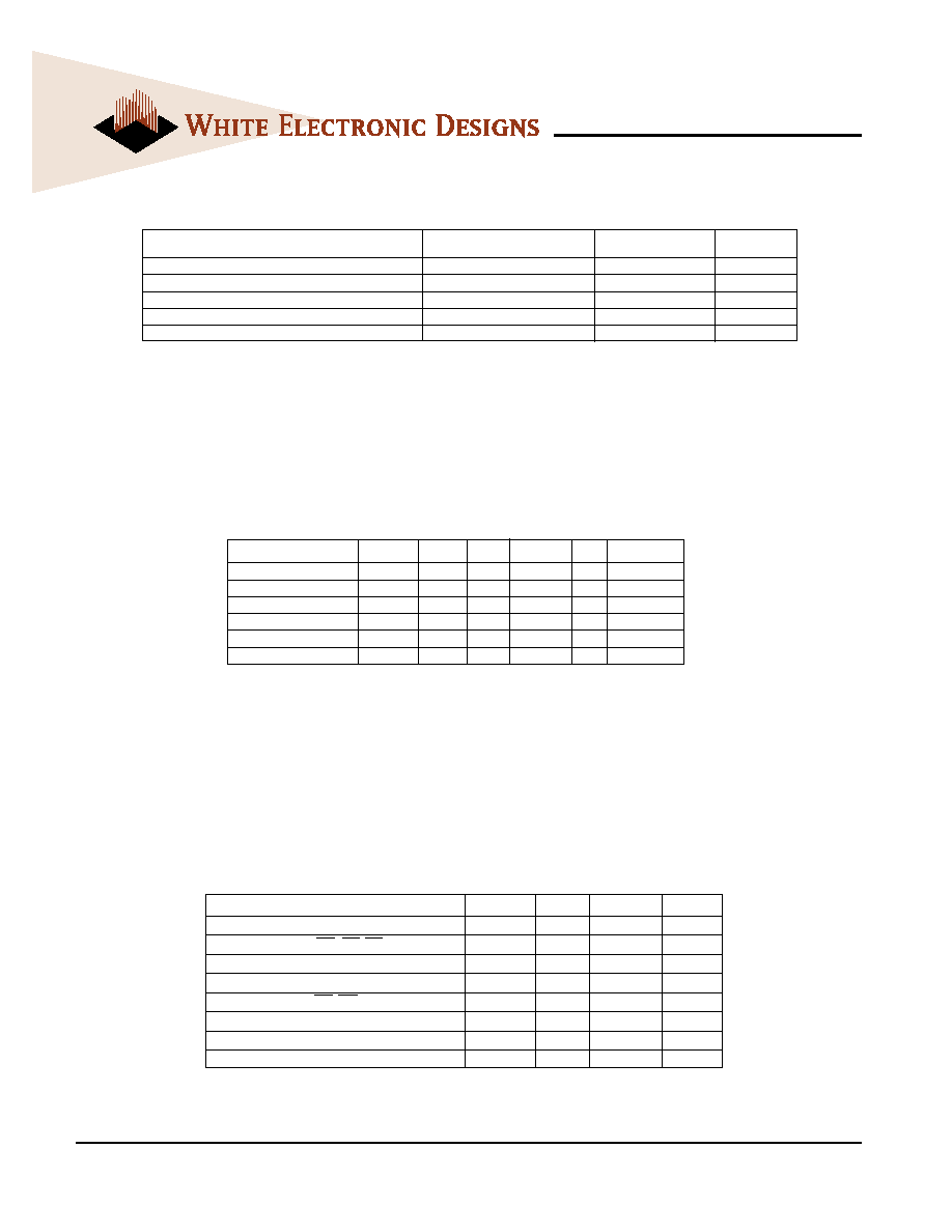
ABSOLUTE MAXIMUM RATINGS
Note: Permanent device damage may occur if "ABSOLUTE MAXIMUM RATINGS" are exceeded.
Functional operation should be restricted to recommended operating condition.
Exposure to higher than recommended voltage for extended periods of time could affect device reliability.
RECOMMENDED DC OPERATING CONDITIONS
Parameter
Symbol
Min
Typ
Max
Unit
Note
Supply Voltage
VDD
3.0
3.3
3.6
V
Input High Voltage
VIH
2.0
3.0 VDDQ+0.3 V
1
Input Low Voltage
VIL
-0.3
0.8
V
2
Output High Voltage
VOH
2.4
V
IOH= -2mA
Output Low Voltage
VOL
0.4
V
IOL= -2mA
Input Leakage Current
ILI
-10
10
µA
3
Note: 1. VIH (max)= 5.6V AC. The overshoot voltage duration is £ 3ns.
2. VIL (min)= -2.0V AC. The undershoot voltage duration is £ 3ns.
3. Any input 0V £ VIN £ VDDQ
Input leakage currents include Hi-Z output leakage for all bi-directional buffers with Tri-State
outputs.
CAPACITANCE
(T
A
= 23∞C, f = 1MHz, V
DD
= 3.3V, VREF=1.4V 6200mV)
Parameter
Symbol
Min
Max
Unit
Input Capacitance (A0-A12)
CIN1
-
85
pF
Input Capacitance (RAS,CAS,WE)
CIN2
-
85
pF
Input Capacitance (CKE0,CKE1)
CIN3
-
45
pF
Input Capacitance (CLK0,CLK1)
CIN4
-
21
pF
Input Capacitance (CS0,CS1)
CIN5
-
25
pF
Input Capacitance (DQM0-DQM7)
CIN6
-
15
pF
Input Capacitance (BA0-BA1)
CIN7
-
85
pF
Data input/output capacitance (DQ0-DQ63)
Cout
-
18
pF
Parameter
Symbol
Value
Units
Voltage on any pin relative to VSS
V
IN
, Vout
-1.0 ~ 4.6
V
Voltage on VDD supply relative to VSS
VDD, VDDQ
-1.0 ~ 4.6
V
Storage Temperature
TSTG
-55 ~ +150 ∞C
Power Dissipation
PD
16
W
Short Circuit Current
IOS
50
mA
4
White Electronic Designs Corporation (508) 485-4000 www.whiteedc.com
June 2003 Rev. 1
ECO #16372
WED3DG6434V-D1
White Electronic Designs Corp reserves the right to change products or specifications without notice.
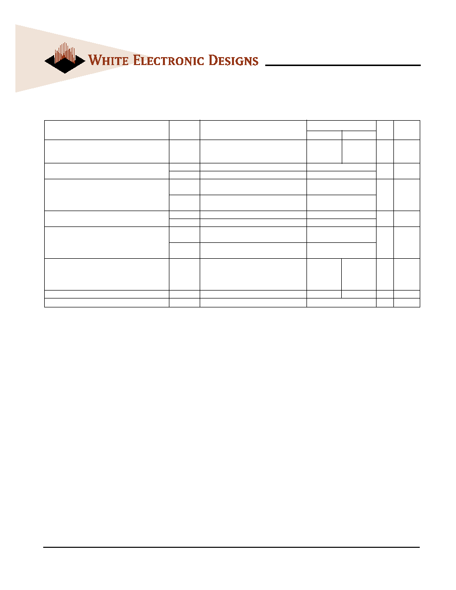
OPERATING CURRENT CHARACTERISTICS
(V
CC
= 3.3V, T
A
= 0∞C to +70∞C)
Notes: 1. Measured with outputs open.
2. Refresh period is 64ms.
3. Unless otherwise noticed, input swing level is CMOS (VIH/VIL = VDDQ/VssQ)
Version
Parameter
Symbol
Conditions
133
100
Units Note
Operating Current
ICC1
Burst Length = 1
1040
960
mA
1
(One bank active)
tRC ≥ tRC(min)
IOL = 0mA
Precharge Standby Current
ICC2P
CKE £ VIL(max), tCC = 10ns
32
mA
in Power Down Mode
ICC2PS
CKE & CLK £ VIL(max), tCC = •
32
Icc2N
CKE ≥ VIH(min), CS ≥ VIH(min), tcc = 10ns
Precharge Standby Current
Input signals are charged one time during 20
320
in Non-Power Down Mode
Icc2NS
CKE ≥ VIH(min), CLK £ VIL(max), tcc = •
mA
Input signals are stable
160
Active standby current in
ICC3P
CKE ≥ VIL(max), tCC = 10ns
80
mA
power-down mode
ICC3PS
CKE & CLK £ VIL(max), tcc = •
80
ICC3N
CKE ≥ VIH(min), CS ≥ VIH(min), tcc = 10ns
Active standby current in
Input signals are changed one time during 20ns 480
mA
non power-down mode
ICC3NS
CKE ≥ VIH(min), CLK £ VIL(max), tcc = •
input signals are stable
400
mA
Io = mA
Operating current (Burst mode)
ICC4
Page burst
1120
1040
mA
1
4 Banks activated
tCCD = 2CLK
Refresh current
ICC5
tRC ≥ tRC(min)
2000
1760
mA
2
Self refresh current
ICC6
CKE £ 0.2V
32
mA
5
White Electronic Designs Corporation (508) 485-4000 www.whiteedc.com
June 2003 Rev. 1
ECO #16372
WED3DG6434V-D1
White Electronic Designs Corp reserves the right to change products or specifications without notice.
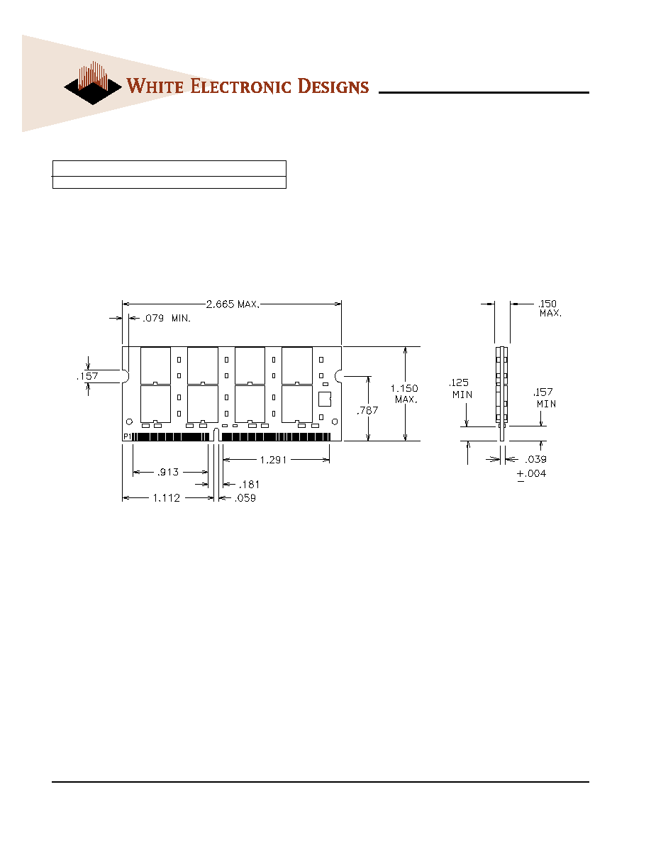
ALL DIMENSIONS ARE IN INCHES
PACKAGE DIMENSIONS
ORDERING INFORMATION
Part Number
Speed
Cas Latency
WED3DG6434V11D1
100MHz
CL=3