
W541L240 Data Sheet
4-BIT MICROCONTROLLER
Publication Release Date: May 29, 2003
- 1 -
Revision A5
Table of Contents-
1.
GENERAL DESCRIPTION ......................................................................................................... 2
2.
FEATURES ................................................................................................................................. 2
3.
BLOCK DIAGRAM ...................................................................................................................... 4
4.
PIN CONFIGURATION............................................................................................................... 5
5.
PIN DESCRIPTION..................................................................................................................... 6
6.
ELECTRICAL CHARACTERISTICS........................................................................................... 7
6.1
Absolute Maximum Ratings .......................................................................................... 7
6.2
DC Characteristics ........................................................................................................ 7
6.3
AC Characteristics......................................................................................................... 8
7.
APPLICATION CIRCUIT............................................................................................................. 9
8.
REVISION HISTORY ................................................................................................................ 10

W541L240
- 2 -
1. GENERAL DESCRIPTION
The W541L240 is fully compatible with W741L240 in the terms of pin assignment and IC functon
except main oscillator. It is a high-performance 4-bit microcontroller (
�C) that provides an LCD driver.
The device contains a 4-bit ALU, a 8-bit timer, a divider, a 24
� 4 LCD driver, and three 4-bit I/O ports
(including 1 output port for LED driving). There are also three interrupt sources and 8-level subroutine
nesting for interrupt applications. The W541L240 operates on low voltage and very low current and
has two power reduction modes, hold mode and stop mode, which help to minimize power dissipation.
The W541L240 is suitable for remote controllers, watches and clocks, multiple I/O products, keyboard
controllers, speech synthesis LSI controllers, and other products.
2. FEATURES
� Operating voltage: 1.2 ~ 1.8V (LCD drive voltage: 3.0V, or 4.5V)
� Crystal/RC oscillation circuit selectable by code option for system clock
� Crystal oscillator: 32.768 KHz only
� RC oscillator: 1 MHz (maximum)
- High-frequency (400 KHz to 1 MHz) or low-frequency (below 400 KHz) oscillation option must
be determined by the code option.
- In RC mode, attention must be paid to the high/low frequency oscillation option, because the
LCD driver frequency is related to this option.
� Memory
- 2048 � 16 bit program ROM (including 2K � 4 bit look-up table)
- 64 � 4 bit data RAM (including 16 working registers)
- 24 � 4 LCD data RAM
� 13 input/output pins
- Ports for input only: 1 port/4 pins
- Input/output ports: 2 ports/8 pins
- MFP output pin: 1 pin (MFP)
- Do not be floating when it is as input or output open-drain (NMOS type).
� Power-down mode
- Hold function: no operation (except for oscillator)
- Stop function: no operation (including main clock)
� Three types of interrupts
- Two internal interrupts (Divider 0, Timer 1)
- One external interrupts (Port RC)

W541L240
Publication Release Date: May 29, 2003
- 3 -
Revision A5
� LCD driver output
- 24 segment � 4 common
- Static, 1/2 duty (1/2 bias), 1/3 duty (1/2 or 1/3 bias), 1/4 duty (1/3 bias) driving mode can be
selected
� MFP output pin
- Output is software selectable as modulating or nonmodulating frequency
- Works as frequency output specified by Timer 1
� Built-in 14-bit clock frequency divider circuit
� One built-in 8-bit programmable countdown timers
- Timer 1: Offers auto-reload function and one of two internal clock frequencies (F
OSC
or F
OSC
/64)
can be selected (output through MFP pin)
� Built-in 18/14-bit watchdog timer selectable for system reset
� Powerful instruction set: 100 instructions
� 8-level subroutine (include interrupt) nesting
� Up to 4 �S instruction cycle (with 1 MHz operating frequency)
� Packaged in 64-pin QFP

W541L240
- 4 -
3. BLOCK DIAGRAM
LCD DRIVER
PC
STACK
(8 Levels)
RAM
(64*4)
ALU
Timing Generator
PORT RA
PORT RC
Modulation
Frequency
Pulse
SEG0 to SEG23
COM0 to COM3
RA0-3
RC0-3
MFP
XIN
XOUT
VDD
VSS
VDD1-3 DH1-2
ROM
(2048*16)
(look_up table
2K*4)
Timer 1
(8 Bit)
ACC
RES
Divider 0
(14 Bit)
HCF
PEF
HEF
IEF
Central Control
Unit
EVF
SEF
PSR0
PR
MR1
.
.
MUL
SEL
+1(+2)
PM0
PM1
.
.
PORT RB
RB0-3

W541L240
Publication Release Date: May 29, 2003
- 5 -
Revision A5
4. PIN CONFIGURATION
51
50
49
48
47 46 45 44 43 42 41 40 39 38 37 36 35 34 33
1
2
3
4
5 6 7 8 9 10 11 12 13 14 15 16 17 18 19
20
21
22
23
24
25
26
27
28
29
30
31
32
52
53
54
55
56
57
58
59
60
61
62
63
64
NC
NC
RC3
RC2
RC1
RC0
RB3
RB1
M
F
P
N
C
/
R
E
S
X
I
N
O
U
T
V
D N N
D C C
D
H
1
D
H
2
V
D
D
SEG18
SEG17
SEG16
SEG15
SEG14
SEG13
SEG12
SEG11
SEG10
N
C
N
C
V
S
S
N
C
N
C
C
O
M
C
O
M
C
O
M
C
O
M
S
E
G
S
E
G
S
E
G
S
E
G
S
E
G
S
E
G
3 2 1 0 0 1 2 3 4 5
N
C
C
C C
N N
N
S S S
E
E E
G G
E
G
2 1 0 9
G
SEG9
SEG8
SEG7
SEG6
RB0
RA3
RA2
RA1
RB2
S
2 2 2 1
S
E
G
3
2
3
V
D
D
2
V
D
D
X
R
A
0
1
W541L240
- 6 -
5. PIN DESCRIPTION
SYMBOL I/O
FUNCTION
XIN I
Input pin for oscillator.
Connected to crystal or resistor to generate system clock by code option.
External 10~20pF capacitor uses to get accurate freq in crystal mode.
XOUT O
Output pin for oscillator.
Connected to crystal or resistor to generate system clock by code option.
20pF capacitor is built in internal for crystal mode...
RA0
-RA3
I/O
Input/Output port.
Input/output mode specified by port mode 1 register (PM1).
RB0
-RB3
I/O
Input/Output port.
Input/output mode specified by port mode 2 register (PM2).
RC0
-RC3
I
4-bit port for input only.
Each pin has an independent interrupt capability. And build-in schmitt
trigger.
MFP
O
Output pin only.
This pin can output modulating or nonmodulating frequency, or Timer 1
clock output specified by mode register 1 (MR1).
RES
I
System reset pin with pull-high resistor.
SEG0
-SEG23
O
LCD segment output pins.
Also can be used as DC output ports specified by code option.
COM0
-COM3
O
LCD common signal output pins.
Static
COM0
COM1
COM2
COM3
Used
Not Used
1/2 Duty
Not Used
Not Used
Not Used
Not Used
1/3 Duty
Not Used
1/4 Duty
Used
Used
Used
Used
Used
Used
Used
Used
Used
The LCD alternating frequency can be selected by code option.
DH1, DH2
I
Connection terminals for voltage doubler (halver) capacitor.
V
DD1
, V
DD2
,
V
DD3
I
Positive (+) supply voltage terminal.
Refer to Functional Description.
V
DD
I
Positive power supply (+).
V
SS
I
Negative power supply (-).
W541L240
Publication Release Date: May 29, 2003
- 7 -
Revision A5
6. ELECTRICAL CHARACTERISTICS
6.1 Absolute Maximum Ratings
PARAMETER RATING
UNIT
Supply Voltage to Ground Potential
-0.3 to +7.0
V
Applied Input/Output Voltage
-0.3 to +7.0
V
Power Dissipation
120
mW
Ambient Operating Temperature
0 to +70
�C
Storage Temperature
-55 to +150
�C
Note: Exposure to conditions beyond those listed under Absolute Maximum Ratings may adversely affect the life and reliability
of the device.
6.2 DC Characteristics
(V
DD
-V
SS
= 1.5V, F
OSC
. = 32.768 KHz, T
A
= 25
� C; unless otherwise specified)
PARAMETER
SYM.
CONDITIONS
MIN.
TYP.
MAX.
UNIT
Op. Voltage
V
DD
- 1.2
-
1.8
V
Op. Current (Crystal type)
I
OP1
No load (Ext-V)
-
4
12
�A
Op. Current (RC type)
I
OP2
No load (Ext-V)
-
35
65
�A
Hold Current (Crystal type)
I
HM1
Hold mode
No load (Ext-V)
- 3 6
�A
Hold Current (RC type)
I
HM2
Hold mode
No load (Ext-V)
- 16 40
�A
Stop Current (Crystal type)
I
SM1
Stop mode
No load (Ext-V)
- 0.1 2
�A
Stop Current (RC type)
I
SM2
Stop mode
No load (Ext-V)
- 0.1 2
�A
Input Low Voltage
V
IL
- V
SS
- 0.3
V
DD
V
Input High Voltage
V
IH
- 0.7
V
DD
-
V
DD
V
MFP Output Low Voltage
V
ML
I
OL
= 0.9mA
-
-
0.3
V
MFP Output High Voltage
V
MH
I
OH
= -0.75mA
1.2
-
-
V
Port RA, RB Output Low Voltage V
ABL
I
OL
= 1.0mA
-
0.2
0.3
V
Port RA, RB Output Hi Voltage
V
ABH
I
OH
= -0.5mA
1.2
1.4
-
V
LCD Supply Current
I
LCD
All Seg. On
-
-
3
�A
W541L240
- 8 -
DC Characteristics, continued
PARAMETER
SYM.
CONDITIONS
MIN.
TYP.
MAX.
UNIT
SEG0
-SEG23 Sink Current
I
OL
V
OL
= 0.05V
V
LCD
= 0.0V
6 - -
�A
SEG0
-SEG23 Drive Current
I
OH
V
OH
= 4.45V
V
LCD
= 4.5V
1.5 - -
�A
Input Port Pull-up Resistor
R
C
Port RC
200
1000
1500
K
RES
Pull-up Resistor
R
RES
- 200
500
1500
K
6.3 AC Characteristics
(V
DD
-V
SS
= 1.5V, T
A
= 25
� C; unless otherwise specified)
PARAMETER
SYM.
CONDITIONS
MIN.
TYP.
MAX.
UNIT
RC type
-
-
1000
Op. Frequency
F
OSC
Crystal type (Option low-
speed type only)
- 32.768 - KHz
Oscillator Start-up Time
T
S
V
DD
= 1.2 V,
F
OSC
= 32.768 KHz
- 1 2
S
Instruction Cycle Time
T
I
One machine cycle
-
4/F
OSC
- mS
Reset Active Width
T
RAW
F
OSC
= 32.768 KHz
1
-
-
�S
Interrupt Active Width
T
IAW
F
OSC
= 32.768 KHz
1
-
-
�S
W541L240
Publication Release Date: May 29, 2003
- 9 -
Revision A5
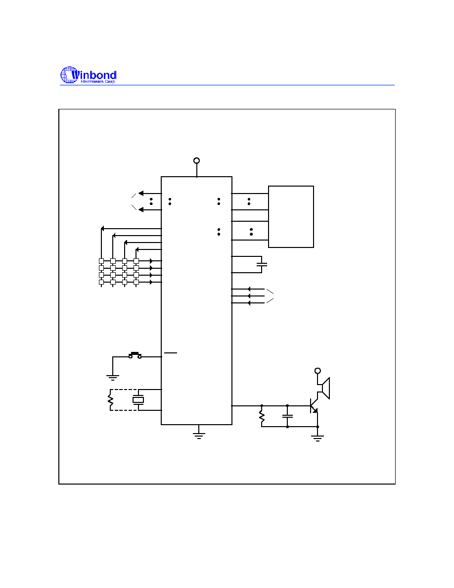
7. APPLICATION CIRCUIT
MFP
RES
XOUT
XIN
DH1
DH2
RC2
RC3
RA0
RA3
Output Signal
RB0
RB1
RB2
COM0
COM3
RB3
RC0
RC1
SEG0
SEG23
or
LCD
PANEL
(1/3 Bias
1/4 Duty)
Connect to capacitor and VDD
to generate LCD voltage
Vcc
Vcc
V
DD
V
DD1
V
DD2
V
DD3
V
SS
W541L240
- 10 -
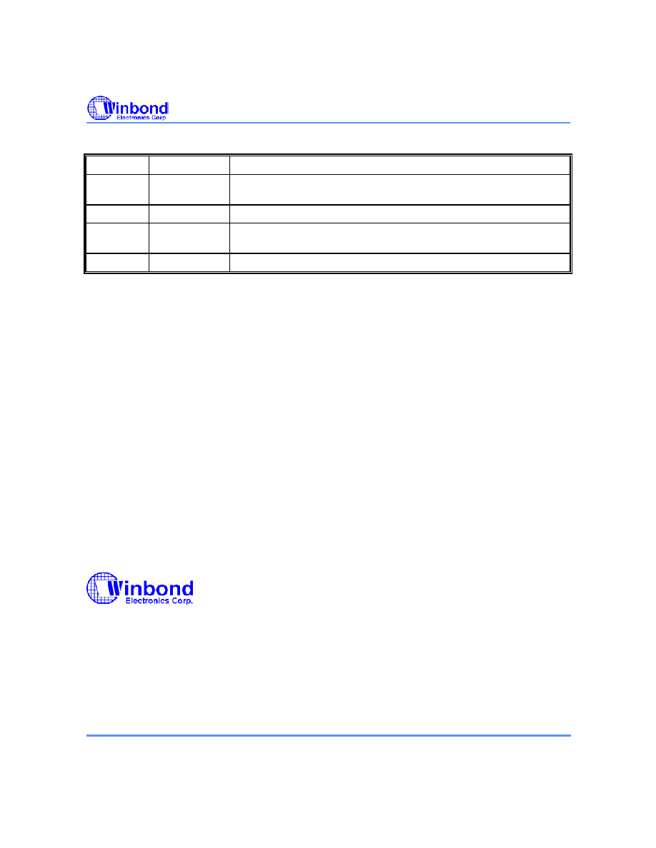
8. REVISION HISTORY
VERSION DATE
DESCRIPTION
A2 -
Note: Recommend working voltage range for Hi freq X all mode
( L series)
A3
-
Note: RC is built-in schmitt trigger
A4 -
Note: Do not be floating when it is as input or output open-drain
(NMOS type)
A5
May 29, 2003
Note : Update DC psec formate
Headquarters
No. 4, Creation Rd. III,
Science-Based Industrial Park,
Hsinchu, Taiwan
TEL: 886-3-5770066
FAX: 886-3-5665577
http://www.winbond.com.tw/
Taipei Office
TEL: 886-2-8177-7168
FAX: 886-2-8751-3579
Winbond Electronics Corporation America
2727 North First Street, San Jose,
CA 95134, U.S.A.
TEL: 1-408-9436666
FAX: 1-408-5441798
Winbond Electronics (H.K.) Ltd.
No. 378 Kwun Tong Rd.,
Kowloon, Hong Kong
FAX: 852-27552064
Unit 9-15, 22F, Millennium City,
TEL: 852-27513100
Please note that all data and specifications are subject to change without notice.
All the trade marks of products and companies mentioned in this data sheet belong to their respective owners.
Winbond Electronics (Shanghai) Ltd.
200336 China
FAX: 86-21-62365998
27F, 2299 Yan An W. Rd. Shanghai,
TEL: 86-21-62365999
Winbond Electronics Corporation Japan
Shinyokohama Kohoku-ku,
Yokohama, 222-0033
FAX: 81-45-4781800
7F Daini-ueno BLDG, 3-7-18
TEL: 81-45-4781881
9F, No.480, Rueiguang Rd.,
Neihu District, Taipei, 114,
Taiwan, R.O.C.