 | –≠–ª–µ–∫—Ç—Ä–æ–Ω–Ω—ã–π –∫–æ–º–ø–æ–Ω–µ–Ω—Ç: W89C940 | –°–∫–∞—á–∞—Ç—å:  PDF PDF  ZIP ZIP |
Document Outline
- Main Menu
- LAN Products
- Search
- Web

W89C940
ELANC-PCI (TWISTED-PAIR ETHER-LAN CONTROLLER WITH
PCI INTERFACE)
GENERAL DESCRIPTION
he ELANC-PCI (Twisted-pair Ether-LAN Controller with PCI Interface) integrates a W89C902 Serial(ELANC-
PCI) LAN Coprocessor for Twisted-Pair (SLCT) and PC/AT PCI bus interface logic into a single chip. The
ELANC-PCI provides an easy way of implementing the interface between an IEEE 802.3-compatible Ethernet
and a personal computer, ELANC-PCI also provide fast DMA operation to improve the packet transmit and
receive performance.
The PCI bus is a high performance local bus architecture with low latency random access time. It is a
synchronous bus with operation up to 33MHz. The PCI bus interface is designed to provide the registers with
the device information required for configuration, recording the status of the lines , control registers, interrupt
line and I/O base address registers. It is capable of functioning in a half-duplex environment.
The W89C940Fis designed to fully comply with the standard of PCI 2.0 specification. Taking advantage of PCI's
nature, W89C940F supports auto-configuration function to free users' depression and confusion on tunning
system resources conflict. With extremely high throughput on PCI bus, W89C940F offers a 32 bits data path to
highly boost its performance without extra cost. Comparing with LAN card with ISA bus, its improvement is
excellent. Besides, it also supports up to 256KB flash memory reserved for various applications, for instance
anti-virus, popular drivers, Boot ROM, viewing your PC assets...etc., and what is more, these software are able
to be updated on line. This can increase more niche feature on your LAN card, help you get more and bright
your company profile. W89C940F is a single chip - build-in PCI bus interface and all necessary circuits - which
will let design and board assembly become easy.
FEATURES
∑ Fully compatible with IEEE 802.3 standard
∑ Software compatible with Novell NE2000
∑ Complies with PCI Local Bus Specification Revision 2.0
∑
Slave Mode for PCI bus
∑
Fast DMA operation enhancing network access performance
∑
AUI, UTP interface available
∑
Supports one chip 32Kx8 and 16Kx8 SRAM
∑
Supports up to 64KB boot ROM
∑ EEPROM auto-load function after power on reset
∑
EEPROM on-board programming function available
∑
UTP interface polarity auto detection correction function available
∑ UTP/BNC auto media-switching function provided
∑
LED displaying for network segment Link/activity status
∑
Signature register available for device identification
∑
Single 5V power supply with low power consumption
∑
100 Pin PQFP

W89C940
2
PIN CONFIGURATION
50
5
1
5
2
5
3
5
4
5
5
5
6
5
7
5
8
5
9
6
0
6
1
6
2
6
3
6
4
6
5
6
6
6
7
6
8
6
9
7
0
7
1
7
2
7
3
7
4
81
7
5
7
6
7
7
7
8
7
9
8
0
82
83
84
85
86
87
88
89
49
48
47
46
45
44
43
42
41
40
39
38
37
36
35
34
90
91
92
93
94
95
96
97
98
99
100
1
2
3
4
5
6
1
0
1
1
7
8
9
1
2
1
3
1
4
1
5
1
6
1
7
1
8
1
9
2
0
2
1
2
2
2
3
2
4
2
5
2
6
2
7
2
8
2
9
3
0
33
32
31
V
C
C
A
D
2
2
A
D
2
1
A
D
2
0
A
D
1
9
A
D
1
8
A
D
1
7
A
D
1
6
A
D
1
5
C
B
E
#
2
/
F
R
A
M
#
E
I
R
D
Y
#
T
R
D
Y
#
D
E
V
S
E
L
#
S
T
O
P
#
G
N
D
V
C
C
P
A
R
C
#
B
E
#
1
A
D
1
4
A
D
1
3
A
D
1
2
A
D
1
1
A
D
1
0
A
D
9
A
D
8
C
/
B
E
#
0
B
U
S
C
L
K
G
N
D
V
C
C
D
N
G
P
X
T
N
X
T
N
X
R
P
D
C
P
X
R
N
D
C
A
C
T
E
E
C
S
B
P
C
S
B
R
C
S
B
M
S
A
1
4
\
L
M
S
A
1
3
M
S
A
1
2
M
S
A
1
1
M
S
A
M
M
1
0
S
A
M
S
A
M
S
A
M
S
A
M
S
A
M
S
A
M
S
A
M
S
A
M
S
A
S
A
9
8
7
6
5
4
3
2
1
0
V
C
C
X
1
X
2
G
N
D
TPDP
TPDM
XRDP
XRDM
DGND
RST#
INTA
AD31
AD30
AD29
AD28
AD27
AD26
AD25
AD24
AD23
C/BE3#
IDSEL
DGND
MSWRB
MSRDB
MSD7
MSD6
MSD5
MSD4
MSD3
MSD2
MSD1
MSD0
AD0
AD1
AD2
AD3
AD4
AD5
AD6
AD7
DGND
DVCC
W89C940(100 PINS)
#
AVCC
D
D
D
D
D
D
D
A
W89C940
3
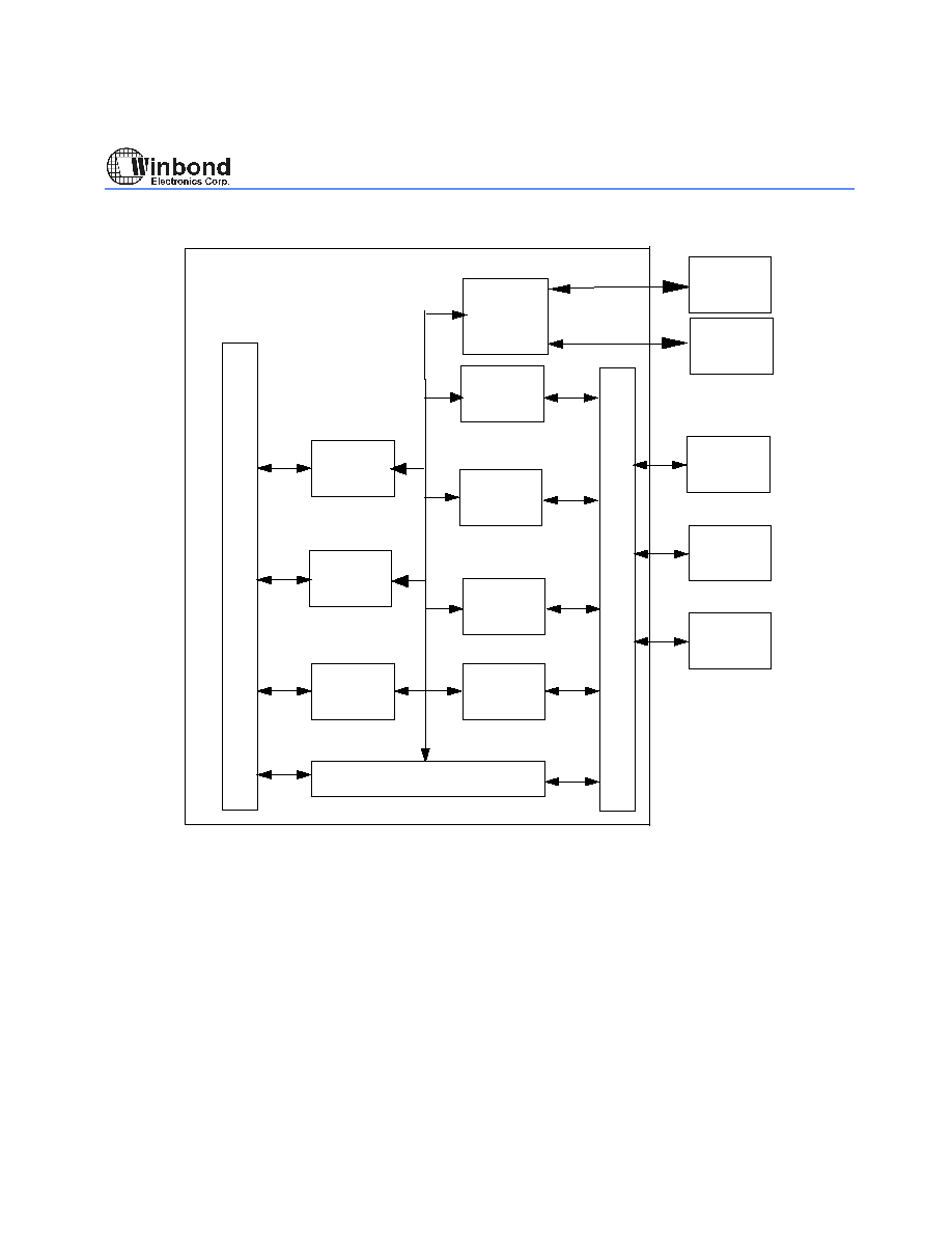
BLOCK DIAGRAM
H
O
S
T
B
U
S
Config.
Registers
Interrupt
Control
Logic
PCI and
Interface
Logic
Local Bus
Arbitrator
Buffer
Memory
Control
EEPROM
Control
Logic
Boot ROM
Control
Logic
B
U
S
SLCT
Module
Data Buffer
M
E
M
O
R
Y
SRAM
BTROM
EEPROM
AUI
TPI

W89C940
4
PIN DESCRIPTION
PCI INTERFACE
NAME
NUMBER
TYPE
DESCRIPTION
CLK
29
in
Clock:
Bus clock from PCI bus. All of the PCI signals, except RST#, are synchronized by
rising edge of clock.
The allowable operating frequency of CLK for W89C940 is from 25MHz to 33MHz.
RST#
87
in
Reset:
Asynchronous reset signal from PCI bus.
AD[31:00]
AD31-
AD24
AD23
AD22-
AD16
AD15-AD8
AD7-AD0
89 - 96
99
2 - 8
19 - 26
33 - 40
t/s
Address and Data:
Bidirection bus for PCI address and data signals transaction. AD[31:00] is a time
division bus. Two phases are used to carry the address and data messages of PCI
bus. The address phase is the clock cycle in which FRAME# is aeerted.
AD[31:24] contains the most significant byte(MSB) and the AD[7:0] contain the least
significant byte(LSB) during the data phase.
The data written from host should be stable and valid when IRDY# is asserted. The
data driven by W89C940 will be stable and valid when TRDY# is asserted.
C/BE[3:0]#
C/BE3#
C/BE2#
C/BE1#
C/BE0#
97
9
18
27
t/s
in
Bus Command and Byte Enables:
C/BE[3:0]# define the type of bus command during the address phase and the byte
enables during the data phase of a transaction. There are 16 types of bus
command defined in PCI bus. Four bits of C/BE[3:0]# are used to decode the 16
types of bus command. The byte enable determine which byte lanes carry
meaningful data.
C/BE0# indicate the byte 0(AD[7:0]) is valid. C/BE1# indicate the byte 1(AD[15:8]) is
valid. C/BE2# indicate the byte 2(AD[23:16]) is valid. C/BE3# indicate the byte
3(AD[32:24]) is valid.
PAR
17
t/s
Parity:
Even parity across AD[31:0] and C_BE[3:0]B.
W89C940 will drive the PAR in read data phase. The host drives the PAR for
address phase and writes data phase. PAR is stable and valid one clock after the
address phase. PAR is stable and valid one clock after either IRDY# is asserted on a
write transaction or TRDY# is asserted on a read transaction. Once PAR is valid, it
remains valid until one clock after the completion of the current data phase.
FRAME#
10
s/t/s
in
Cycle Frame:
FRAME# is asserted by host to indicate the beginning of a bus transaction. When
FRAME# is deasserted, the transaction is in the final data phase.

W89C940
5
PCI INTERFACE
NAME
NUMBER
TYPE
DESCRIPTION
IRDY#
11
s/t/s
in
Initiator Ready:
Initiator Ready indicates the host's ability to complete the current data phase of
transaction. During a write cycle, IRDY# indicates that valid data is presented on
AD[31:00]. During a read cycle, it indicates the master is ready to accept the
data. The wait cycles are inserted till IRDY# and TRDY# are asserted at the
same cycle.
TRDY#
12
s/t/s
Target Ready:
Target Ready indicates the W89C940's ability to complete the current data phase
of transaction. During a read cycle, TRDY# indicates that valid data is presented
on AD[31:00]. During a write cycle, it indicates the W89C940 is ready to accept
the data. The wait cycles are inserted till both IRDY# and TRDY# are asserted at
the same cycle.
STOP#
14
s/t/s
STOP:
Stop indicates W89C940 is requesting the master to stop the current transaction.
IDSEL
98
in
Initialization Device Select:
IDSEL is used as a chip select during PCI configuration read and write
transaction.
DEVSEL#
13
s/t/s
Device Select:
DEVSEL# will be asserted when W89C940 decode the correct address.
INTA#
88
o/d
Interrupt Request:
INTA# is used to request an interrupt service. The interrupt signal can be
masked by the register of IMR( Interrupt Mask Register). INTA# status is kept at
ISR( Interrupt Status Register).
NETWORK INTERFACE
NAME
NUMBER
TYPE
DESCRIPTION
X1
X2
53
52
I/TTL
O/TTL
Crystal or Oscillator Input.
Crystal or oscillator input (X1) and output (X2) pin. If a crystal is used, it should
be connected directly to X1 and X2. If an oscillator is selected, X1 is the 20 MHz
input and X2 should be left floating.
TXP
TXN
75
74
O/AUI
AUI Transmit Output:
AUI differential output pair. The data transmitted by DTE will be sent through TXP
and TXN in a differential signal with manchest code format. A 270 ohm pull-down
resistor is required for each of TXP and TXN. TXP and TXN should be isolated
by a pulse transformer from directly connecting outside loop.