 | –≠–ª–µ–∫—Ç—Ä–æ–Ω–Ω—ã–π –∫–æ–º–ø–æ–Ω–µ–Ω—Ç: W986432DH | –°–∫–∞—á–∞—Ç—å:  PDF PDF  ZIP ZIP |
Document Outline
- Main Menu
- Memory Products
- Search
- Web

PRELIMINARY W986432DH
512K
◊
◊
4 BANKS
◊
◊
32 BITS SDRAM
Publication Release Date: May 2000
- 1 - Revision A0
GENERAL DESCRIPTION
W986432DH is a high-speed synchronous dynamic random access memory (SDRAM), organized as
512K words
◊
4 banks
◊
32 bits. Using pipelined architecture and 0.175
µ
m process technology,
W986432DH delivers a data bandwidth of up to 800M bytes per second (5). For different application,
W986432DH is sorted into four speed grades: -5, -55, -6, -7,-8.
Accesses to the SDRAM are burst oriented. Consecutive memory location in one page can be
accessed at a burst length of 1, 2, 4, 8 or full page when a bank and row is selected by an ACTIVE
command. Column addresses are automatically generated by the SDRAM internal counter in burst
operation. Random column read is also possible by providing its address at each clock cycle. The
multiple bank nature enables interleaving among internal banks to hide the precharging time.
By having a programmable Mode Register, the system can change burst length, latency cycle,
interleave or sequential burst to maximize its performance. W986432DH is ideal for main memory in
high performance applications.
FEATURES
∑
3.3V ±0.3V power supply
∑
524288 words
◊
4 banks
◊
32 bits organization
∑
Auto Refresh and Self Refresh
∑
CAS latency: 2 and 3
∑
Burst Length: 1, 2, 4, 8, and full page
∑
Sequential and Interleave burst
∑
Burst read, single write operation
∑
Byte data controlled by DQM
∑
Power-down Mode
∑
Auto-precharge and controlled precharge
∑
4K refresh cycles/64 mS
∑
Interface: LVTTL
∑
Packaged in 86-pin TSOP II, 400 mil - 0.50

PRELIMINARY W986432DH
512K
◊
◊
4 BANKS
◊
◊
32 BITS SDRAM
Publication Release Date: May 2000
- 2 - Revision A0
PIN CONFIGURATION
86
84
83
82
81
80
79
78
77
76
75
74
73
72
71
70
69
68
67
66
65
64
63
62
61
60
59
1
2
3
4
5
6
7
8
9
10
11
12
13
14
15
16
17
18
19
20
21
22
23
24
25
26
27
37
38
39
40
41
42
43
28
29
30
31
32
33
34
35
36
50
49
48
47
46
45
44
58
57
56
55
54
53
52
51
85
V
ss
DQ15
V
SS
Q
DQ14
DQ13
V
CC
Q
DQ12
DQ11
V
SS
Q
DQ10
DQ9
V
CC
Q
DQ8
NC
V
SS
DQM1
NC
NC
CLK
CKE
A9
A8
A7
A6
A5
A4
A3
DQM3
V
SS
NC
DQ31
V
CC
Q
DQ30
DQ29
V
SS
Q
DQ28
DQ27
V
CC
Q
DQ26
DQ25
V
SS
Q
DQ24
V
SS
VCC
DQ0
V
CC
Q
DQ1
DQ2
V
SS
Q
DQ3
DQ4
V
CC
Q
DQ5
DQ6
VSSQ
DQ7
NC
VCC
DQM0
WE
CAS
RAS
CS
NC
BS0
BS1
A10/AP
A0
A1
A2
DQM2
V
CC
NC
DQ16
V
SS
Q
DQ17
DQ18
V
CC
Q
DQ19
DQ20
V
SS
Q
DQ21
DQ22
V
CC
Q
DQ23
V
CC
PIN DESCRIPTION
PIN NAME
FUNCTION
DESCRIPTION
A0
-
A10
Address
Multiplexed pins for row and column address.
Row address: A0
-
A10. Column address: A0
-
A7.
A10 is sampled during a precharge command to determine if
all banks are to be precharged or bank selected by BS0, BS1.
BS0, BS1
Bank Select
Select bank to activate during row address latch time, or bank
to read/write during address latch time.
DQ0
-
DQ31
Data Input/
Output
Multiplexed pins for data output and input.
CS
Chip Select
Disable or enable the command decoder. When command
decoder is disabled, new command is ignored and previous
operation continues.
RAS
Row Address
Strobe
Command input. When sampled at the rising edge of the
clock
RAS
,
CAS
and
WE
define the operation to be
executed.
CAS
Column Address
Strobe
Referred to
RAS
WE
Write Enable
Referred to
RAS

W986432DH
Publication Release Date: May 2000
- 3 - Revision A0
DQM0
-
DQM3
Input/output mask The output buffer is placed at Hi-Z (with latency of 2) when
DQM is sampled high in read cycle. In write cycle, sampling
DQM high will block the write operation with zero latency.
CLK
Clock Inputs
System clock used to sample inputs on the rising edge of
clock.
CKE
Clock Enable
CKE controls the clock activation and deactivation. When
CKE is low, Power Down mode, Suspend mode, or Self
Refresh mode is entered.
V
CC
Power (+3.3V)
Power for input buffers and logic circuit inside DRAM.
V
SS
Ground
Ground for input buffers and logic circuit inside DRAM.
V
CCQ
Power (+3.3V) for
I/O buffer
Separated power from V
CC
, to improve DQ noise immunity.
V
SSQ
Ground for I/O
buffer
Separated ground from V
SS
, to improve DQ noise immunity.
NC
No Connection
No connection
W986432DH
- 4 -
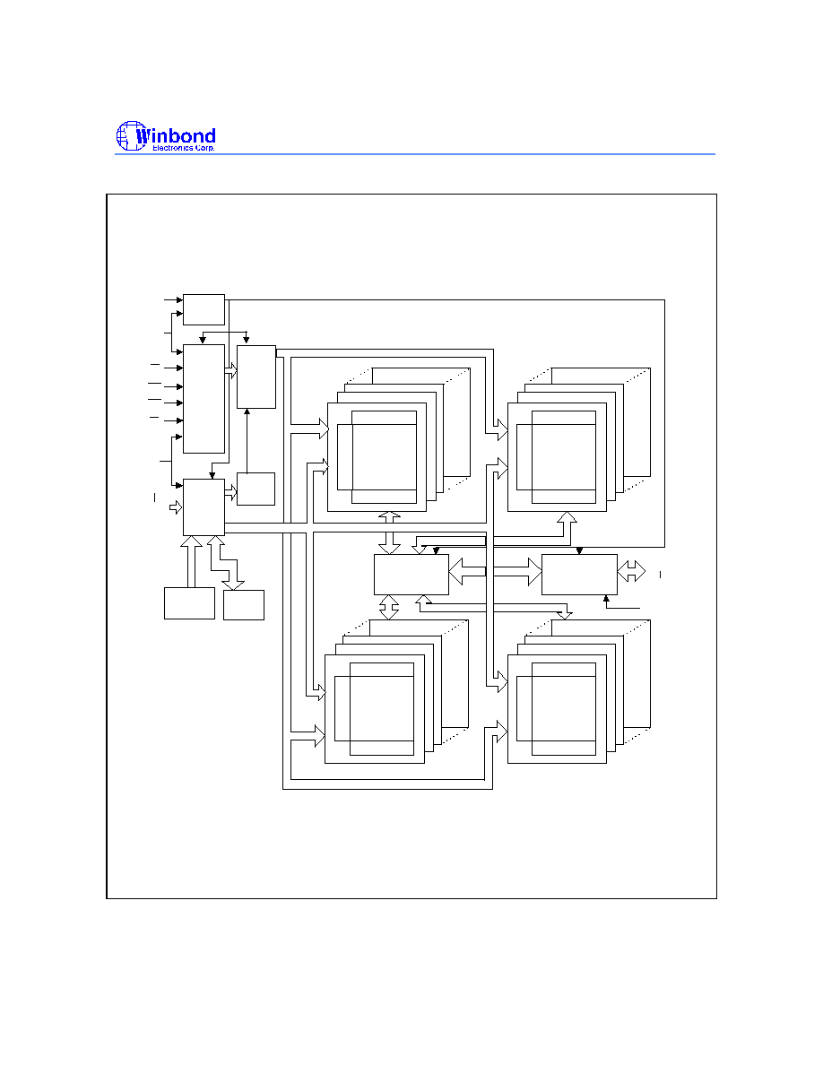
BLOCK DIAGRAM
DQ0
DQ31
DQM0~3
CLK
CKE
A10
CLOCK
BUFFER
COMMAND
DECODER
ADDRESS
BUFFER
REFRESH
COUNTER
COLUMN
COUNTER
CONTROL
SIGNAL
GENERATOR
MODE
REGISTER
COLUMN DECODER
SENSE AMPLIFIER
CELL ARRAY
BANK #2
COLUMN DECODER
SENSE AMPLIFIER
CELL ARRAY
BANK #0
COLUMN DECODER
SENSE AMPLIFIER
CELL ARRAY
BANK #3
DATA CONTROL
CIRCUIT
DQ
BUFFER
COLUMN DECODER
SENSE AMPLIFIER
CELL ARRAY
BANK #1
NOTE:
The cell array configuration is 2048 * 256 * 32
ROW DECODER
ROW DECODER
ROW DECODER
ROW DECODER
A0
A9
BS0
BS1
CS
RAS
CAS
WE
W986432DH
Publication Release Date: May 2000
- 5 - Revision A0
DC CHARACTERISTICS
Absolute Maximum Rating
PARAMETER
SYM.
RATING
UNIT
NOTES
Input, Column Output Voltage
V
IN
, V
OUT
-0.3
-
V
CC
+0.3
V
1
Power Supply Voltage
V
CC,
V
CCQ
-0.3
-
4.6
V
1
Operating Temperature
T
OPR
0
-
70
∞
C
1
Storage Temperature
T
STG
-55
-
150
∞
C
1
Soldering Temperature (10s)
T
SOLDER
260
∞
C
1
Power Dissipation
P
D
1
W
1
Short Circuit Output Current
I
OUT
50
mA
1
Note: Exposure to conditions beyond those listed under Absolute Maximum Ratings may adversely affect the life and reliability of the
device.
RECOMMENDED DC OPERATING CONDITIONS
(T
A
= 0 to 70
∞
C)
PARAMETER
SYM.
MIN.
TYP.
MAX.
UNIT
NOTE
S
Power Supply Voltage
V
CC
3.0
3.3
3.6
V
2
Power Supply Voltage (for I/O
Buffer)
V
CCQ
3.0
3.3
3.6
V
2
Input High Voltage
V
IH
2.0
-
V
CC
+0.3
V
2
Input Low Voltage
V
IL
-0.3
-
0.8
V
2
Note: V
IH
(max.) = V
CC
/V
CC
Q+1.2V for pulse width < 5 nS
V
IL
(min.) = V
SS
/V
SS
Q-1.2V for pulse width < 5 nS
CAPACITANCE
(V
DD
= 3.3V, T
A
= 25
∞
C, f = 1 MHz)
PARAMETER
SYM.
MIN.
MAX.
UNIT
Input Capacitance
(A0 to A11, BS0, BS1,
CS
,
RAS
,
CAS
,
WE
, DQM, CKE)
C
i
2.5
4
pf
Input Capacitance (CLK)
C
CLK
2.5
4
pf
Input/Output capacitance (DQ0
-
DQ31)
C
o
4
6.5
pf
Note: These parameters are periodically sampled and not 100% tested
W986432DH
- 6 -
DC CHARACTERISTICS
(V
CC
= 3.3V
±
0.3V, T
A
= 0
∞
~70
∞
C)
PARAMETER
SYM.
-5
-55
-6
-7
-8
UNIT
NOTES
MAX.
MAX.
MAX.
MAX.
MAX.
Operating Current
t
CK
= min., t
RC
= min.
Active precharge command
cycling without burst
operation
1 bank
operation
I
CC1
TBD
TBD
TBD
TBD
TBD
3
Standby Current
t
CK
= min., CS = V
IH
V
IH/L
= V
IH
(min.)/V
IL
(max.)
CKE = V
IH
I
CC2
TBD
TBD
TBD
TBD
TBD
3
Bank: inactive state
CKE = V
IL
(Power Down
mode)
I
CC2P
TBD
TBD
TBD
TBD
TBD
3
Standby Current
CLK = V
IL
, CS = V
IH
V
IH/L
=V
IH
(min.)/V
IL
(max.)
CKE = V
IH
I
CC2S
TBD
TBD
TBD
TBD
TBD
BANK: inactive state
CKE = V
IL
(Power Down
mode)
I
CC2P
S
TBD
TBD
TBD
TBD
TBD
mA
No Operating Current
t
CK
= min., CS = V
IH
(min.)
CKE = V
IH
I
CC3
TBD
TBD
TBD
TBD
TBD
BANK: active state (4 banks)
CKE = V
IL
(Power Down
mode)
I
CC3P
TBD
TBD
TBD
TBD
TBD
Burst Operating Current (t
CK
= min.)
Read/Write command cycling
I
CC4
TBD
TBD
TBD
TBD
TBD
3, 4
Auto Refresh Current (t
CK
= min.)
Auto refresh command cycling
I
CC5
TBD
TBD
TBD
TBD
TBD
3
Self Refresh Current (CKE = 0.2V)
Self refresh mode
I
CC6
TBD
TBD
TBD
TBD
TBD
PARAMETER
SYMBOL
MIN.
MAX.
UNIT
NOTES
Input Leakage Current
(0V
V
IN
V
CC
, all other pins not under test = 0V)
I
I
(L)
-5
5
µ
A
Output Leakage Current
7(Output disable, 0V
V
OUT
V
CC
Q)
V
O
(L)
-5
5
µ
A
LVTTL Output
H
Level Voltage
(I
OUT
= -2 mA)
V
OH
2.4
-
V
LVTTL Output
"
L
Level Voltage
(I
OUT
= 2 mA)
V
OL
-
0.4
V
W986432DH
Publication Release Date: May 2000
- 7 - Revision A0
AC CHARACTERISTICS
(V
CC
= 3.3V
±
0.3V, V
SS
= 0V, Ta = 0 to 70
∞
C) (Notes: 5, 6.)
PARAMETER
Symbol
-5
-55
-6
UNIT NOTE
MIN
MAX
MIN
MAX
MIN
MAX
Ref/Active to Ref/Active Command Period tRC
54
55
60
ns
Active to precharge Command Period
tRAS
40
100000 40
100000 42
100000
Active to Read/Write Command Delay Time tRCD
14
15
18
Read/Write(a) to Read/Write(b)Command
Period
tCCD
1
1
1
Cycle
Precharge to Active(b) Command Period tRP
14
15
18
ns
Active(a) to Active(b) Command Period
tRRD
10
10.8
12
Write Recovery Time
CL* = 2
tWR
7
7.5
7.5
CL* = 3
5
5.4
6
CLK Cycle Time
CL* = 2
tCK
7
1000
7.5
1000
7.5
1000
CL* = 3
5
1000
5.4
1000
6
1000
CLK High Level
tCH
2
2
2
CLK Low Level
tCL
2
2
2
Access Time from CLK
CL* = 2
tAC
4.5
5.5
5.5
CL* = 3
4.5
5
5
Output Data Hold Time
tOH
2.75
2.75
2.75
Output Data High Impedance Time
tHZ
2.75
5
2.75
5.4
2.75
6
Output Data Low Impedance Time
tLZ
0
0
0
Power Down Mode Entry Time
tSB
0
5
0
5.4
0
6
Transition Time of CLK (Rise and Fall)
tT
0.5
10
0.5
10
0.5
10
Data-in-Set-up Time
tDS
1
1.5
1.5
Data-in Hold Time
tDH
0.5
0.5
0.5
Address Set-up Time
tAS
1.3
1.5
1.5
Address Hold Time
tAH
0.8
1
0.5
CKE Set-up Time
tCKS
1.3
1.5
1.5
CKE Hold Time
tCKH
0.8
1
0.5
Command Set-up Time
tCMS
1
1.5
1.5
Command Hold Time
tCMH
0.5
0.5
0.5
Refresh Time
tREF
64
64
64
ms
Mode Register Set Cycle Time
tRSC
10
10.8
12
ns

W986432DH
- 8 -
AC CHARACTERISTICS
(V
CC
= 3.3V
±
0.3V, V
SS
= 0V, Ta = 0 to 70
∞
C) (Notes: 5, 6.)
PARAMETER
Symbol
-7
-8
UNIT NOTE
MIN
MAX
MIN
MAX
MIN
MAX
Ref/Active to Ref/Active Command Period tRC
65
68
ns
Active to precharge Command Period
tRAS
45
100000 48
100000
Active to Read/Write Command Delay Time tRCD
20
20
Read/Write(a) to Read/Write(b)Command
Period
tCCD
1
1
Cycle
Precharge to Active(b) Command Period
tRP
20
20
ns
Active(a) to Active(b) Command Period
tRRD
14
20
Write Recovery Time
CL* = 2
tWR
7.5
10
CL* = 3
7
8
CLK Cycle Time
CL* = 2
tCK
7.5
1000
10
1000
CL* = 3
7
1000
8
1000
CLK High Level
tCH
2
3
CLK Low Level
tCL
2
3
Access Time from CLK
CL* = 2
tAC
5.5
6
CL* = 3
5
6
Output Data Hold Time
tOH
3
3
Output Data High Impedance Time
tHZ
3
7
3
8
Output Data Low Impedance Time
tLZ
0
0
Power Down Mode Entry Time
tSB
0
7
0
8
Transition Time of CLK (Rise and Fall)
tT
0.5
10
0.5
10
Data-in-Set-up Time
tDS
0.5
2
Data-in Hold Time
tDH
1
1
Address Set-up Time
tAS
0.5
2
Address Hold Time
tAH
1
1
CKE Set-up Time
tCKS
0.5
2
CKE Hold Time
tCKH
1
1
Command Set-up Time
tCMS
0.5
2
Command Hold Time
tCMH
1
1
Refresh Time
tREF
64
64
ms
Mode Register Set Cycle Time
tRSC
14
16
ns

W986432DH
Publication Release Date: May 2000
- 9 - Revision A0
PACKAGE DIMENSIONS
86L TSOP (II)-400 mil
SEATING PLANE
E
D
A2
A1
A
b
ZD
1
43
86
44
e
H
E
Y
L
C
L1
q
ZD
0.61
0.024
0.002
0.007
MAX.
MIN.
NOM.
A2
b
A
A1
0.17
1.00
0.05
0.27
1.20
0.15
SYM.
DIMENSION
(MM)
MAX.
MIN.
NOM.
e
0.50
0.020
0.016
L
0.40
0.50
0.60
0.020
0.024
0.396
E
10.06
10.16
10.26
0.400
0.404
0.871
D
22.22
22.12
22.62
0.875
0.905
0.039
0.011
0.047
0.006
DIMENSION
(INCH)
L1
0.80
0.032
c
0.12
0.005
0.455
11.76
11.56
11.96
0.463
0.471
H
E
Y
0.10
0.004
Controlling Dimension: Millimeters
0.21
0.008

W986432DH
- 10 -
Headquarters
No. 4, Creation Rd. III,
Science-Based Industrial Park,
Hsinchu, Taiwan
TEL: 886-3-5770066
FAX: 886-3-5796096
http://www.winbond.com.tw/
Voice & Fax-on-demand: 886-2-27197006
Taipei Office
11F, No. 115, Sec. 3, Min-Sheng East Rd.,
Taipei, Taiwan
TEL: 886-2-27190505
FAX: 886-2-27197502
Winbond Electronics (H.K.) Ltd.
Rm. 803, World Trade Square, Tower II,
123 Hoi Bun Rd., Kwun Tong,
Kowloon, Hong Kong
TEL: 852-27513100
FAX: 852-27552064
Winbond Electronics North America Corp.
Winbond Memory Lab.
Winbond Microelectronics Corp.
Winbond Systems Lab.
2727 N. First Street, San Jose,
CA 95134, U.S.A.
TEL: 408-9436666
FAX: 408-5441798
Note: All data and specifications are subject to change without notice.

This datasheet has been download from:
www.datasheetcatalog.com
Datasheets for electronics components.