
W9960CF
Winbond Confidential 1 June 1997
W9960CF
VIDEO CODEC
Technical Reference Manual
Version 1.11
June, 1997

W9960CF
Winbond Confidential
2
June 1997
Copyright by Winbond Electronics Corp., all rights reserved
The information in this document has been carefully checked and is believed to be correct as of
the date of publication. Winbond Electronics Corp. reserves the right to make changes in the
product or specification, or both, presented in this publication at any time without notice.
Winbond assumes no responsibility or liability arising from the specification listed herein.
Winbond makes no representations that the use of its products in the manner described in this
publication will not infringe on existing or future patent, trademark, copyright, or rights of third
parties. No license is granted by implication or other under any patent or patent rights of
Winbond Electronics Corp.
IBM is a registered trademark and AT, XT, and OS/2 are trademarks of International Business
Machines Corp.
Intel is a registered trademark of Intel Corporation.
Microsoft is a registered trademark and Windows, Windows 95, and DirectDraw are trademarks
of Microsoft Corp.
Philips is a registered trademark of Philips International B.V.
A
LL OTHER TRADEMARKS AND REGISTERED TRADEMARKS ARE THE PROPERTY OF THEIR RESPECTIVE HOLDERS
.

W9960CF
Winbond Confidential
3
June 1997
1. INTRODUCTION ..................................................................................................... 5
1.1 O
VERVIEW
................................................................................................................. 5
1.2 F
EATURES
.................................................................................................................. 6
2. PIN DESCRIPTION.................................................................................................. 7
2.1 P
IN
D
EFINITION
.......................................................................................................... 7
2.2 P
IN
O
UT
D
IAGRAM
.................................................................................................... 11
3. FUNCTIONAL DESCRIPTION ............................................................................ 12
3.1 W9960CF A
RCHITECTURE
....................................................................................... 12
3.2 PCI I
NTERFACE
........................................................................................................ 13
3.3 VRISC .................................................................................................................... 14
3.4 F
RAME
M
EMORY
DMA C
ONTROLLER
( FDMA ) ...................................................... 20
3.4.1 Bus Arbitration ................................................................................................. 21
3.4.2 FDMA Transfer Type ........................................................................................ 21
3.4.3 FDMA Programming ........................................................................................ 22
3.4.4 FDMA Addressing Registers ............................................................................. 24
3.5 E
XTERNAL
M
EMORY
DMA C
ONTROLLER
( XDMA )................................................ 26
3.6 DRAM M
EMORY
I
NTERFACE
................................................................................... 28
3.7 INTERRUPT/TRIGGER C
ONTROLLER
................................................................... 30
3.8 X_INTERRUPT C
ONTROLLER
( XINTC ) ............................................................... 32
3.9 GPIO ( G
ENERAL
P
URPOSE
I
NPUT
/O
UPUT
) P
ORT
..................................................... 33
3.10 TIMER.................................................................................................................. 33
3.11 V
IDEO
P
RE
/P
OST
P
ROCESSING
E
NGINE
................................................................... 35
3.11.1 Video PreProcessor (VPRE)............................................................................ 35
3.11.2 Video PostProcessor (VPOST)......................................................................... 36
3.12 M
OTION
E
STIMATION
E
NGINE
................................................................................ 38
3.13 FILTER E
NGINE
.................................................................................................... 39
3.14 FIDCT/Q/IQ E
NGINE
............................................................................................. 42
3.15 P
ROGRAMMABLE
I
NPUT
/O
UTPUT
E
NGINE
............................................................... 44
3.16 V
ARIABLE
L
ENGTH
C
ODE
D
ECODER
....................................................................... 46
3.17 A
UDIO
C
OPROCESSOR
I
NTERFACE
.......................................................................... 47
3.18 V
ARIABLE
L
ENGTH
C
ODE
E
NCODING
(VLE) E
NGINE
.............................................. 48
3.19 ISA-
LIKE
I
NTERFACE
.............................................................................................. 49
4. W9960CF REGISTERS .......................................................................................... 51
4.1 PCI C
ONFIGURATION
R
EGISTERS
.............................................................................. 51
5. ELECTRICAL SPECIFICATIONS....................................................................... 57
5.1 A
BSOLUTE
M
AXIMUM
R
ATINGS
................................................................................ 57

W9960CF
Winbond Confidential
4
June 1997
5.2 DC S
PECIFICATIONS
................................................................................................. 57
5.3 AC S
PECIFICATIONS
................................................................................................. 57
5.3.1 Clock Specification ........................................................................................... 58
5.3.2 Reset Timing ..................................................................................................... 58
5.3.3 PCI Interface AC Timing................................................................................... 59
5.3.4 AUDIO Interface AC Timing............................................................................. 60
5.3.5 DRAM Interface AC Timing .............................................................................. 61
5.3.6 GPIO AC Timing............................................................................................... 62
5.3.7 Video PreProcessor AC Timing......................................................................... 63
5.3.8 ISA-Like Bus AC Timing ................................................................................... 64
6. APPENDIXES ......................................................................................................... 65
6.1 P
ORTING
G
UIDE FOR
W9960 W
IN
95 D
EVICE
D
RIVER
............................................... 65
6.2 F
IRMWARE
L
OADING
P
RECEDURE
............................................................................ 65
6.3 A
PPLICATION
/F
IRMWARE
C
OMMAND
B
LOCK
............................................................ 65
W9960CF
Winbond Confidential 5 June 1997
1. INTRODUCTION
1.1 Overview
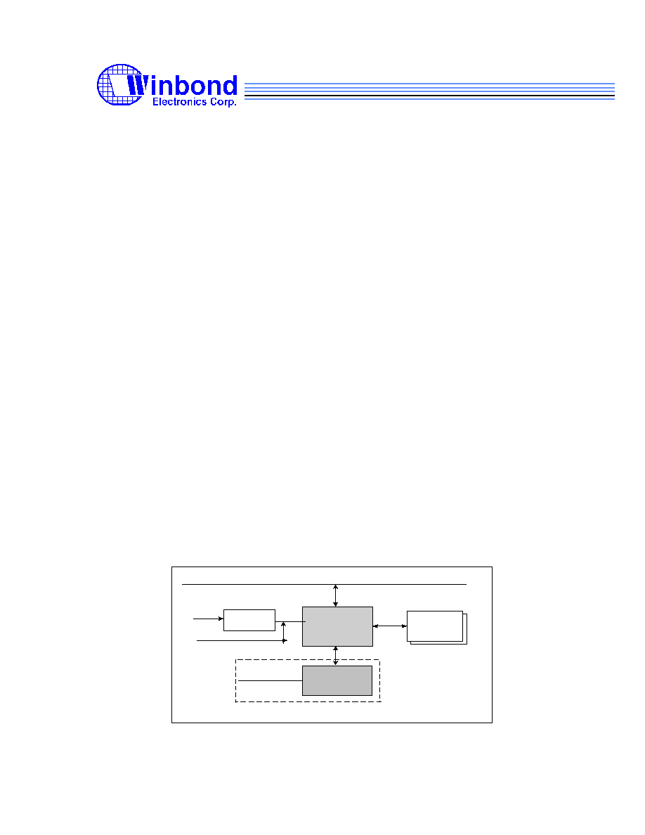
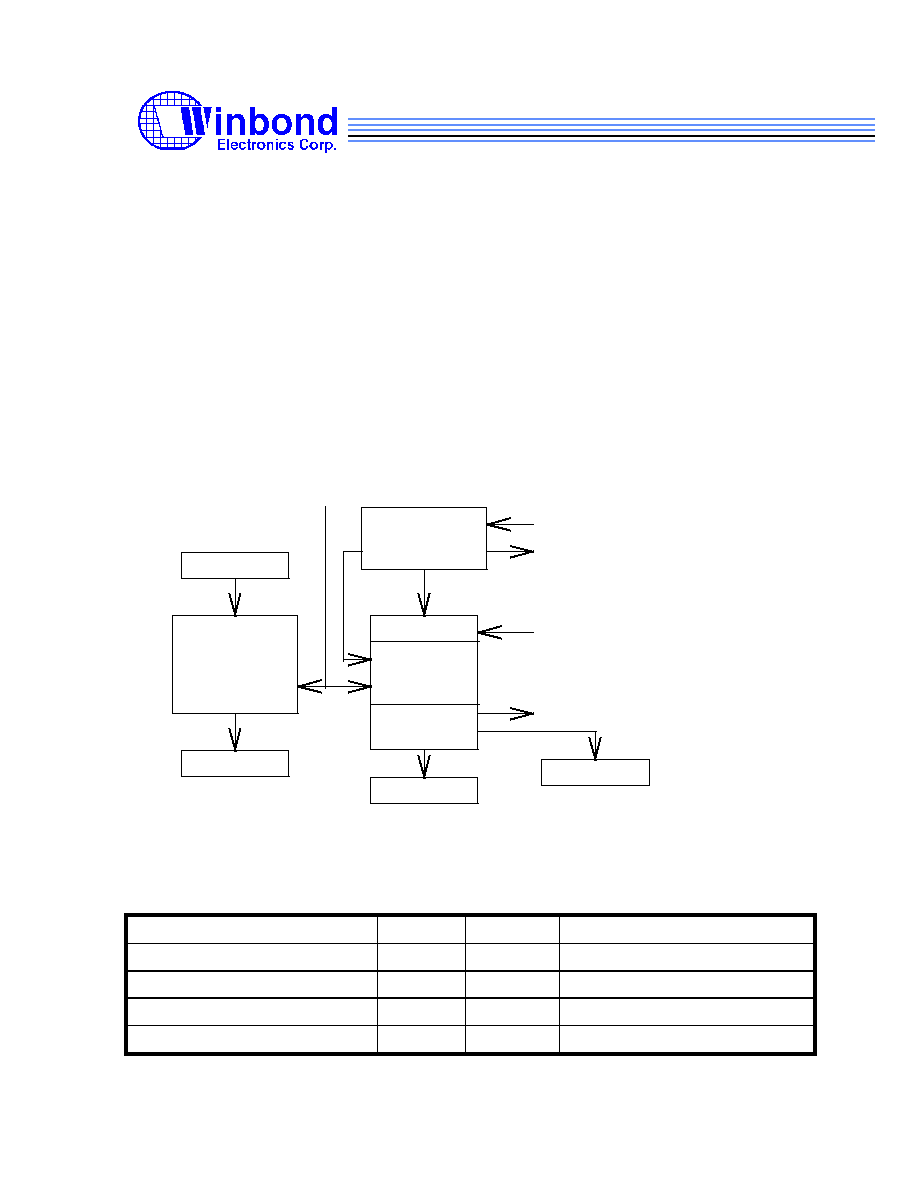
W9960CF is a single chip multi-protocol high performance video CODEC offered by Winbond
Electronics Corp. for video compression and decompression applications such as video-
conference.
W9960CF is composed of a high performance RISC processor core (VRISC), function blocks for
video encoding/decoding and a downloadable program memory such that the system can be run-
time configured for a variety of video applications. The function blocks in W9960CF are
computing engines for: Discrete Cosine Transform (DCT), Inverse Discrete Cosine Transform
(IDCT), Motion Estimation (ME), Motion Compensation (MC), Quantization (Q), Dequantization
(Q
-1
) and VLE/VLD (Variable Length Encoding/Decoding) algorithms. Using these function
blocks, the firmware can direct the VRISC processor to perform ITU-T H.261/ H.263
simultaneous video bitstream encoding/decoding.
Although W9960CF is designed for multiple standard video encoding and decoding, it is
particularly optimized for H.261/H.263 video-conference application. W9960CF supports all
video resolutions as specified in the H.261/H.263 standards, including SQCIF, QCIF and CIF
at high video frame rate. For CIF resolution in H.261 and QCIF resolution in H.263,
specifically, W9960CF delivers excellent encoding/decoding performance.
Implementing most the advanced video encoding options, W9960CF enables lowest video
data rate such that maximum frame rate can be achieved through ISDN, PSTN and Internet
networks. The advanced encoding options supported are: Unrestricted Motion Vector Mode, and
PB-frame Mode. With half-pixel search for motion estimation function, W9960CF further
enhances video quality with even lowered video bitstream data rate.
W9960CF is also designed with a most cost-effective PC based video-conference solution in
mind. It has a digital live video interface for glueless support a of major video decoders and
coefficient-programmable filter circuitry for input video enhancement. For video displaying, it
supports PCI master mode capability to access video frame buffer of PCI-based graphics
adapters. W9960CF also provides an interface for audio modules. The audio modules connected
can be a CODEC for G.711/G.722/G.723/G.728 standards, or a PCM CODEC for audio raw
data. W9960CF uses ordinary FPM or EDO DRAM as working storage. Figure shows application
block diagram.
P C I B u s
256x16
D R A M
W 9 9 6 0
V i d e o C O D E C
V i d e o
D e c o d e r
Audio
C O D E C
V i d e o C a m e r a
M ic/Spk
( O p t i o n a l )
D i g i t a l C a m e r a

W9960CF
Winbond Confidential 6 June 1997
1.2 Features
�
Built-in RISC processor core and 4.5Kx22 bits program memory
�
Supports ITU-T H.263 and H.261 simultaneous video encoding and decoding
�
Supports SQCIF, QCIF and CIF video resolutions
�
Supports H.263 Annex D Unrestricted Motion Vector mode
�
Supports H.263 Annex G PB-frames Mode
�
Supports both integer search and half-pixel search motion estimation
�
Built-in BCH error correction and framing error detection circuitry
�
Supports YUV 4:2:2 video input interface for video camera
�
Built-in filter circuit with programmable coefficients for input video enhancement
�
Selectable video output formats including YUV 4:2:2 and RGB 5:6:5
�
Supports PCI master mode to access graphics adapters for video displaying
�
Supports panning and zooming over video input
�
Provides audio connection to external audio DSP modules
�
Uses conventional FPM and EDO DRAM
�
No SRAM required
�
Optimized for 3.3 volts operation
�
0.5um CMOS technology
�
208-pin PQFP package
W9960CF
Winbond Confidential 7 June 1997
2. PIN DESCRIPTION
2.1 Pin Definition
Pin Name Pin No. Type Function
PCI BUS (50 pins)
AD31-AD0 204-205,4-9,
16-23, 42-49,
57-60, 65-68
IO Address and Data are multiplexed on the same PCI pins. The
address phase is the clock cycle in which FRAME# is
asserted. During data phase AD7-AD0 contain the least
significant byte (lsb) and AD31-AD24 contain the most
significant byte (msb)
C/BE3-C/BE0 14,28,37,56 IO Bus Command and Byte Enables are multiplexed on the
same PCI pins. During the address phase of a transaction,
C/BE3#-C/BE0# define the bus command. During the data
phase C/BE3#-C/BE0# are used as Byte Enable
PAR 36 IO Parity is even parity across AD31-AD0 and C/BE3#-C/BE0#
FRAME# 29 IO FRAME# is asserted to indicate a bus transaction is beginning
TRDY# 31 IO Target Ready indicates the ability of target agent to complete
the current data phase of the transaction
IRDY# 30 IO Initiator Ready indicates the ability of bus master to complete
the current data phase of the transaction.
INTA# 199 O Interrupt A is used to request an interrupt
STOP# 33 IO Stop indicates the current target is requesting the master to
stop the current transaction.
DEVSEL# 32 IO Device Select, indicates the driving device has decoded its
address as the target of the current access
IDSEL 15 I Initialization Device Select is used as chip select during
configuration read and write transactions.
PERR# 34 IO Parity Error is for the reporting of data parity errors
SERR# 35 O System Error is for reporting address parity errors, or any
other system error where the result will be catastrophic.
REQ# 203 O Request indicates to the arbiter that W9960 desires use of the
bus
GNT# 202 I Grant indicates that W9960 access to the bus has been
granted
CLK 201 I PCI Clock
RST# 200 I PCI Reset
W9960CF
Winbond Confidential
8
June 1997
GPIO BUS (4 pins)
GPIO3-
GPIO0
153, 160-162
IO
Connect to GPIO bus to video decoder or coprocessor
Pin Name
Pin No.
Type
Function
DRAM BUS (50 pins)
MD31-MD0
141-132,127-
118, 113-108,
101-96
IO
DRAM Data Bus
OE1# -OE0#
74,70
O
DRAM Output Enable
RAS1# -
RAS0#
81,73
O
DRAM Row Address Strobes
CAS1# -
CAS0#
80,72
O
DRAM Column Address Strobes
MA9 - MA0
91-82
O
DRAM Address Bus
WE1# -WE0# 75,71
O
DRAM Write Enable; WE1# for MD31-MD16,
and WE0# for MD15-MD0
AUDIO BUS ( 5 pins )
RFS
148
IO
Receiver Frame Signal
TFS
149
IO
Transmission Frame Signal
DT
150
O
Transmission Data
DR
151
I
Receiver Data
SCLK
152
IO
clock of serial port
VIDEO BUS ( 20 pins )
VD15-VD0
186-184, 179-
169, 164-163
I
Video Data Bus
HS/HRESET# 187
IU
Horizontal Sync
VS/VRESET# 188
I
Vertical Sync
HREF/ACTive 189
I
Active region
Dvalid
193
IU
Video Data Valid

W9960CF
Winbond Confidential
9
June 1997
Pin Name
Pin No.
Type
Function
ISA-Like BUS ( 30 pins )
SADATA0 -
SADATA7
196-197, 207,
25-26, 54, 62-
63,
IO
8-bit Parallel Data Bus
SAADDR0 -
SAADDR15
77-78, 93-94,
103, 106, 115-
116, 129-130,
143-144, 155,
158, 166-167
O
16-bit Parallel Address Bus
SAIOR#
181
O
IO Read Control signal
SAIOW#
182
O
IO Write Control signal
EINT1#
192
IU
External Interrupt #1
EINT2#
208
IU
External Interrupt #2
BTEN#
190
IU
External Boot ROM Enable
When BTEN# low active, firmware down-load by through ISA-
Like Bus automatically after RST# inactive
BTFLAG#
191
O
External Boot ROM Chip Select
CLOCK SOURCE ( 2 pins )
CLK_MEM
69
I
Internal Clock
CLK_Video
194
I
Video Clock
Note: IU : Input with internal pull-high Pad

W9960CF
Winbond Confidential 10 June 1997
Pin Name Pin No. Type Function
POWER ( 39 pins )
VDD 1,10,24,38,53,
61,76,92,105,
114,128,142,
157,165,180,
195
3.3V DC Power supply
VSS 3,13,27,41,50,
55,64,79,95,
102,
107,117,131,
145, 154, 159,
168, 183, 198,
206
Ground
VDD5V 52,104,156 5.0V DC Power supply
NC ( 8 pins )
NC 2,11,12, 39,
40, 51, 146,
147
No Connection
W9960CF
Winbond Confidential
11
June 1997
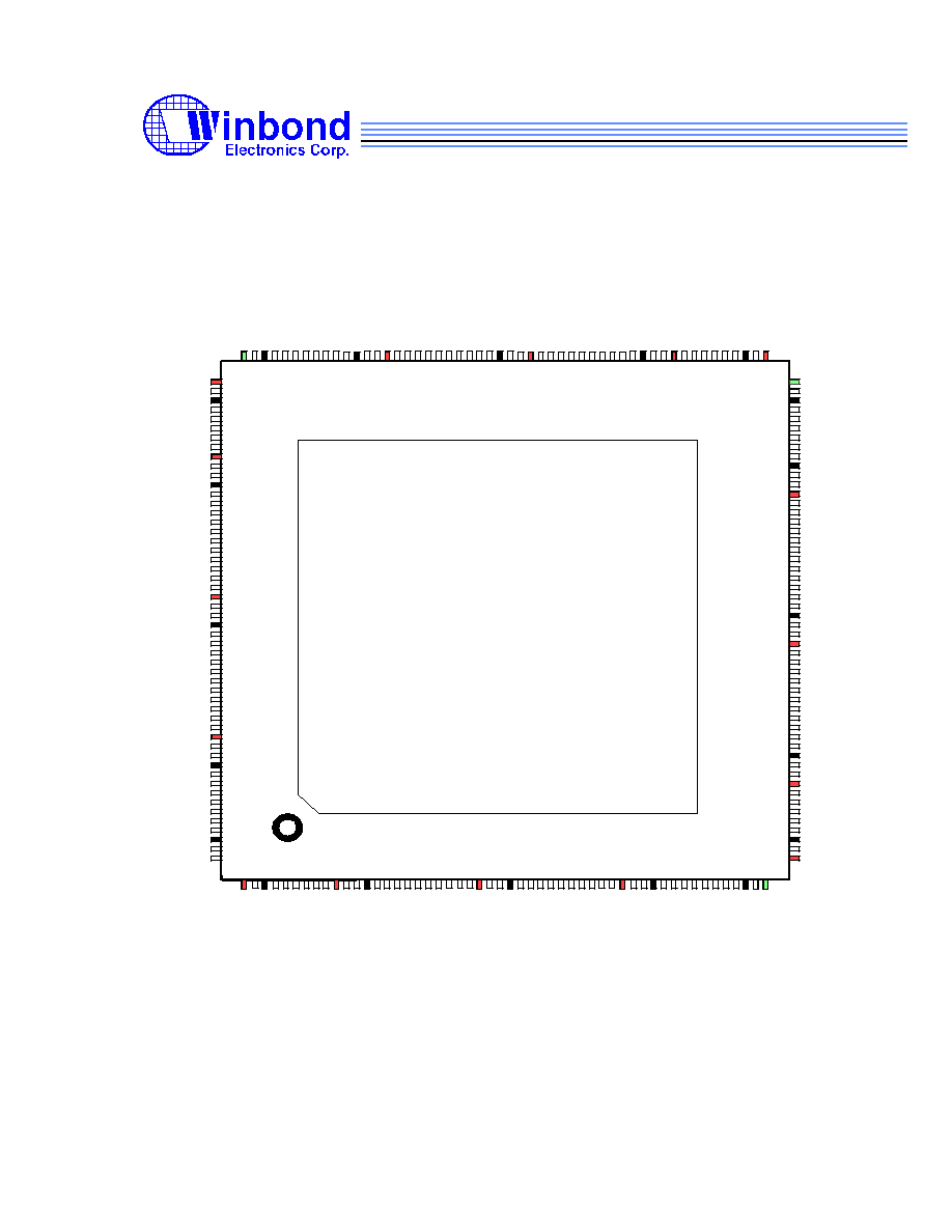
2.2 PinOut Diagram
W9960CF
Video CODEC
BTFLAG#
EINT1#
VDDB
SAADDR14
SAADDR15
VSSB
AD31
AD30
REQ#
GNT#
CLK
RST#
INTA#
CLK_Video
Dvalid
BTEN#
ACTive
VRESET#
HRESET#
VD13
VD14
VD15
VD8
VD9
VD10
VD11
VD12
VD2
VD3
VD4
VD5
VD6
VD7
GPIO2
GPIO1
GPIO0
VD0
VD1
VDDB
SADATA0
SADATA1
VSSB
VDDI
SAIOR#
SAIOW#
VSSI
VDDI
SAADDR13
VSSI
VSSI
SADATA2
EINT2#
VSSB
SADATA7
SADATA6
VDDB
VSSI
SAADDR1
SAADDR0
VDDI
VSSB
SAADDR3
SAADDR2
VDDB
AD4
AD5
AD6
AD7
AD0
AD1
AD2
AD3
MD5
MD4
MD3
MD2
MD1
MD0
MA9
MA8
MA7
MA6
MA5
MA4
MA3
MA2
MA1
MA0
RAS1#
CAS1#
WE0#
OE0#
CLK_MEM
WE1#
OE1#
RAS0#
CAS0#
C/BE0#
VSSI
SADATA5
VDDI
VDD5V
SAADDR4
VSSB
1
5
0
1
5
5
1
4
5
1
4
0
1
3
5
1
3
0
1
2
5
1
2
0
1
1
5
1
1
0
1
0
5
100
95
90
85
80
75
70
65
60
55
160
165
170
175
180
185
190
195
200
205
V
D
D
5
V
S
C
L
K
D
R
D
T
T
F
S
R
F
S
N
C
N
C
V
D
D
B
V
S
S
B
M
D
3
1
V
S
S
B
G
P
I
O
3
M
D
3
0
M
D
2
9
M
D
2
8
M
D
2
7
M
D
2
6
M
D
2
5
M
D
2
4
M
D
2
3
M
D
2
2
V
D
D
I
V
S
S
I
M
D
2
1
M
D
2
0
M
D
1
9
M
D
1
8
M
D
1
7
M
D
1
6
M
D
1
5
M
D
1
4
M
D
1
3
M
D
1
2
M
D
1
1
M
D
1
0
V
D
D
B
V
S
S
B
M
D
9
M
D
8
M
D
7
M
D
6
V
S
S
I
V
D
D
I
S
A
A
D
D
R
1
2
S
A
A
D
D
R
1
0
S
A
A
D
D
R
1
1
S
A
A
D
D
R
9
S
A
A
D
D
R
8
S
A
A
D
D
R
7
S
A
A
D
D
R
6
S
A
A
D
D
R
5
1
0
1
5
2
0
2
5
3
0
3
5
4
0
4
5
5
0
C
/
B
E
1
#
C
/
B
E
2
#
C
/
B
E
3
#
F
R
A
M
E
#
A
D
2
9
V
D
D
B
I
D
S
E
L
I
R
D
Y
#
T
R
D
Y
#
D
E
V
S
E
L
#
S
T
O
P
#
P
E
R
R
#
S
E
R
R
#
P
A
R
A
D
2
8
A
D
2
3
A
D
2
7
A
D
2
6
A
D
2
5
A
D
1
6
A
D
2
4
V
S
S
B
V
D
D
I
V
S
S
I
A
D
2
2
A
D
2
1
A
D
2
0
A
D
1
9
A
D
1
8
A
D
1
7
V
D
D
B
V
S
S
B
A
D
1
5
A
D
1
3
A
D
1
4
A
D
1
2
A
D
1
1
A
D
1
0
A
D
9
A
D
8
V
S
S
B
V
D
D
5
V
V
D
D
I
V
S
S
B
S
A
D
A
T
A
3
S
A
D
A
T
A
4
N
C
N
C
N
C
N
C
N
C
N
C
1
5
W9960CF
Winbond Confidential
12
June 1997
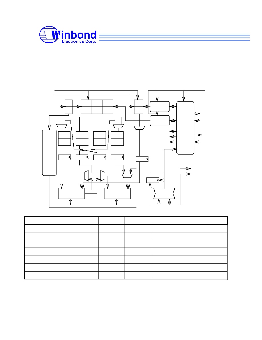
3. FUNCTIONAL DESCRIPTION
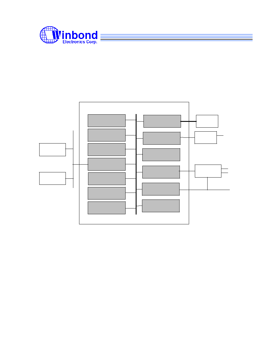
3.1 W9960CF Architecture
W9960CF is composed of a high performance RISC processor core (VRISC), function blocks for
video encoding/decoding and a downloadable program memory such that the system can be run-
time configured for a variety of video applications. The figure is a block diagram for W9960CF.
DSP
ISDN
Modem
Graphics
Adapter
DRAM
PCI Bus
Interface
PCI Memory
DMA Controller
Video Pre/post
Processor
Filter
DCT/IDCT
Q/IQ
DRAM
Controller
PCI_BUS
Video
Decoder
Camera
Speaker
VLE/VLD/BCH
W9960CF
Mic
ISA-Like
Frame Memory
DMA Controller
RISC
Motion
Estimation
Audio Port
Controller
Timer/GPIO
Interrupt Controller
W9960CF
Winbond Confidential
13
June 1997
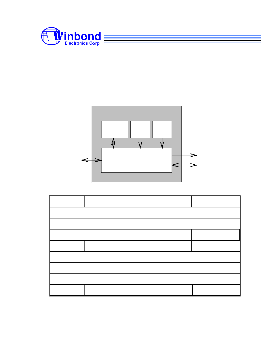
3.2 PCI Interface
W9960CF provides PCI master/slave Interface. In the master mode, it supports fast DMA data
transfer for video/audio bitstream, picture direct draw to graphic display device and VRISC
firmware download. In the slave mode, there are two Base Address Registers for W9960CF
internal registers and external DRAM accessing by the host processor. All data accessing, except
for configuration registers, should be word (2-byte) or double word (4-byte) read/write operations.
CONF
MASCTL
SLACTL
DATAPATH
Internal CPU Bus
Internal XDMA Bus
External PCI Bus
PCI Interface
Address \ Bit
31 24
23 16
15 8
7 0
00H
Device ID
Vendor ID
04H
Status
Command
08H
Class Code
Revision ID
0CH
Reserved
Header Type
Latency Timer
Reserved
10H
Base Address Register 0 (BAR0)
14H
Base Address Register 1 (BAR1)
18H - 38H
Reserved
3CH
Reserved
Reserved
Interrupt Pin
Interrupt Line

W9960CF
Winbond Confidential
14
June 1997
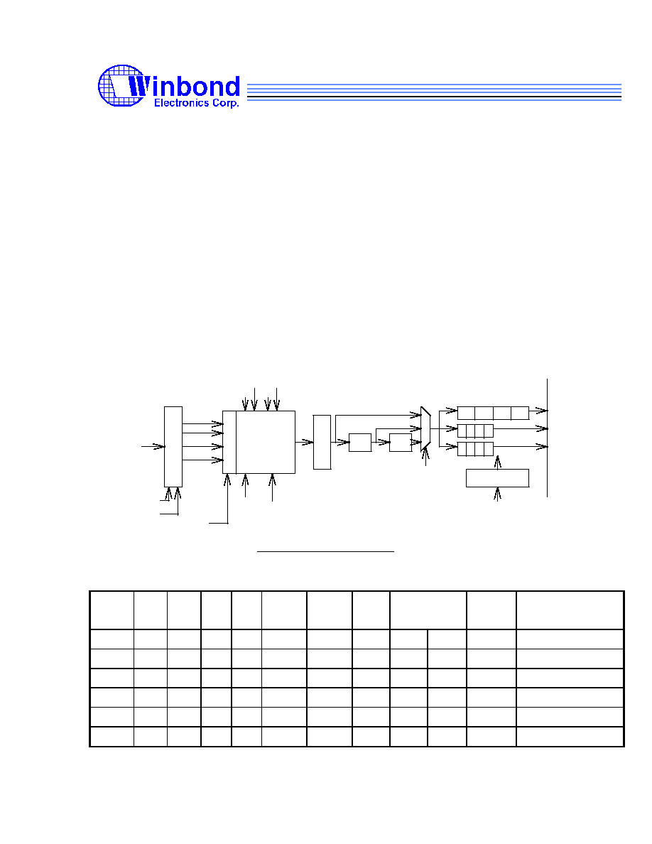
3.3 VRISC
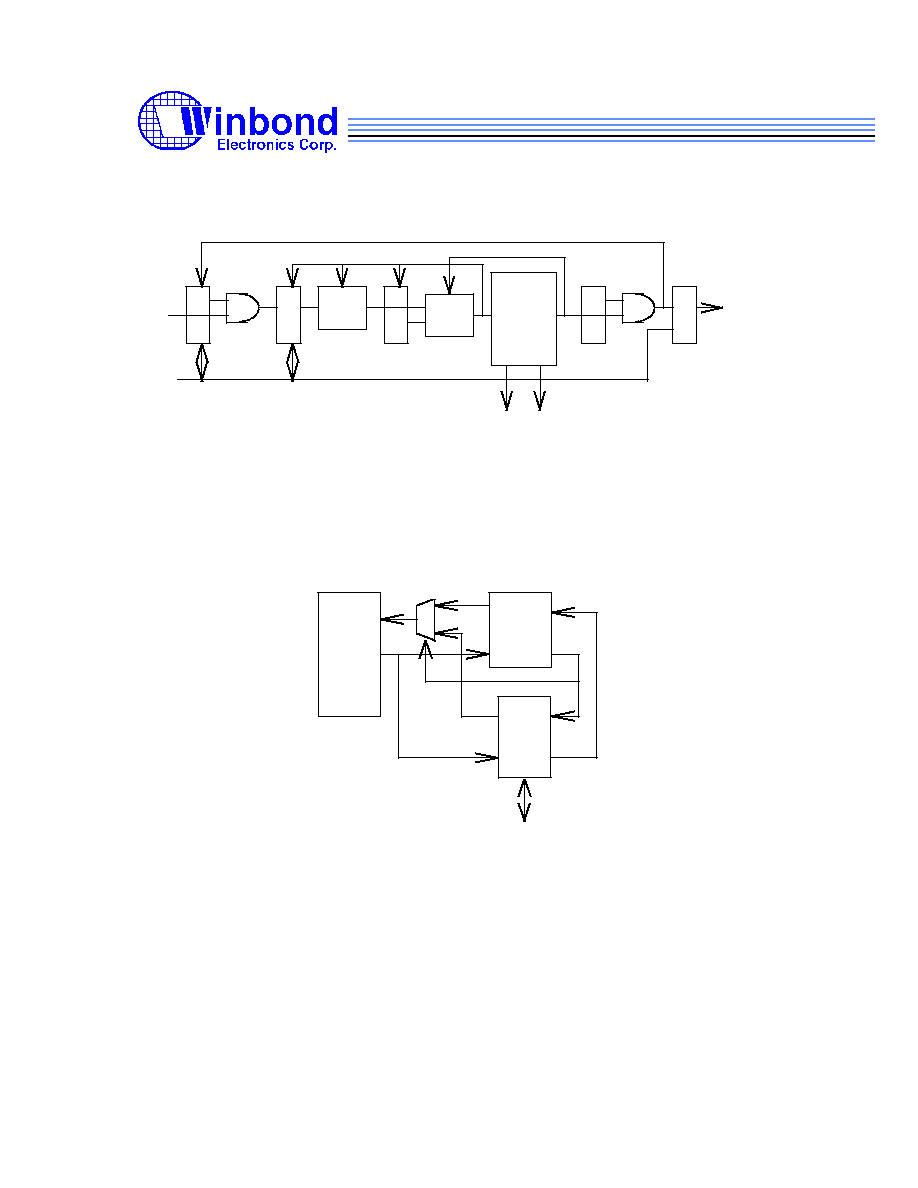
VRISC contains a 4-staged pipeline: Instruction Fetch (IF), Instruction Decoding (DEC),
Operand Execution (EXE), and Result Write-Back (WB), and a 16-bit ALU with Integer
Multiplication and Division. It uses a built-in 1K-byte Data RAM and a 4.5Kx22 bit Instruction
RAM to which the firmware program can be downloaded from the host processor. This VRISC
contains a tri-port (2-read/1-write) 32x16 bit Register File and 32 interrupt vectors.
Interrupt
control
Program
Counter
control
IRAM
control
Instruction
RAM
Decoder
Exec. Inst. Reg.
wp
rp
Arbiter
WB Inst. Reg. 1
WB Inst. Reg. 2
mux
src1
mux
src2
Register
File
imm
ALU
mux
mux
Decoding Inst. Reg.
int1
int8
Instruction
Fetch
Decoding
Execution
Write
Back
RISC Bus
mux
ALU Result Reg.
Address Spaces
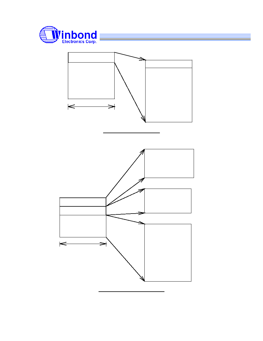
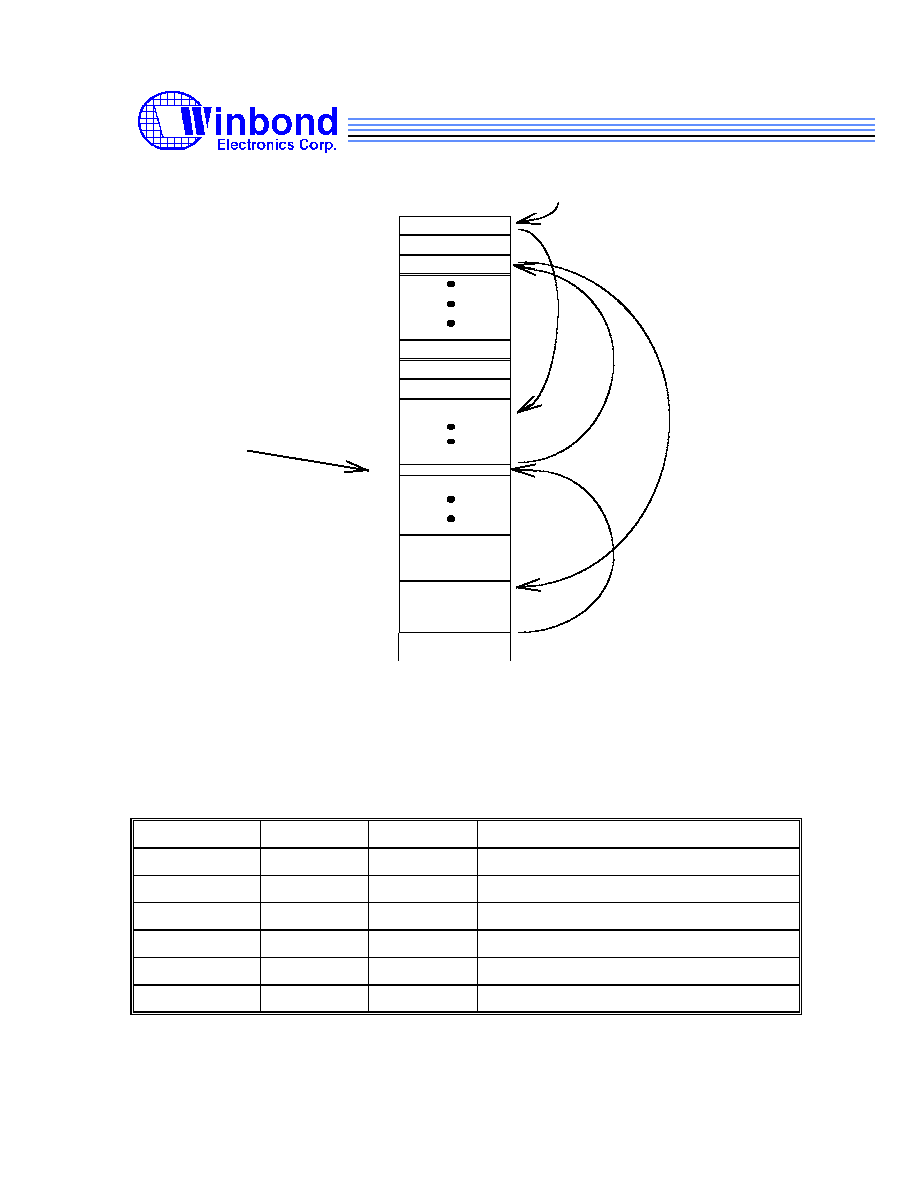
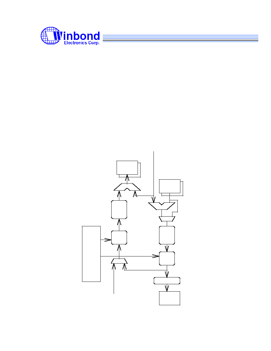
VRISC has two address spaces: the Program Address Space and the Data Memory Address
Space. The following figure illustrates the layout of the booting address, interrupt vector address
space in the main program address space. Program always start from booting address ( 0000H )
after the host enables VRISC. Address 0001H through 001FH stores Interrupt vector for
Interrupt service routines. Figure 2 illustrates the layout of the registers, Data Memory (DM),
external DRAM address space in the main data memory address space. Address 000000H
through 0001FFH is for VRISC Register File referencing, address 000200H through 0003FFH is
for internal DM memory accessing, and address 000400H through 1FFFFFH is for external
DRAM accessing. VRISC cannot access the external DRAM from address 000000H through
0003FFH since this address space are reserved for internal registers and DM memory.
W9960CF
Winbond Confidential
15
June 1997
Program
Address
Space
22bits
0000H
11FFH
Booting
Interrupt
Vector
Address
Space
0000H
0001H
001FH
Program Addressing Space
Data
M e m o r y
Address
S p a c e
(2M)
16bit
0 0 0 0 0 0 H
1 F F F F F H
Engine
Register
Address
S p a c e
(512)
0 0 0 0 0 0 H
0 0 0 1 F F H
D M
Address
S p a c e
(512)
0 0 0 2 0 0 H
0 0 0 3 F F H
D R A M
Address
S p a c e
0 0 0 4 0 0 H
1 F F F F F H
Data Memory Addressing Space
W9960CF
Winbond Confidential
16
June 1997
Addressing Mapping
VRISC has a 5-bit segment register, DMSA. The 21-bit memory address is composed of the 5-
bit content of the DMSA and the content of one of the 32 16-bit general registers as specified in
the Load and Store instruction. The segment register provides a solution to extend the address
space from 64K to 2M bytes. DMSA is a write-only register which can be programmed by the
SEGS imm5 instruction ( see VRISC Instruction Set).
Data Memory Address Mapping
20 16
15 0
DMSA[4:0]
R#[15:0]
General Registers (R0..R31)
VRISC has 32 16-bit general registers to provide the resource for all computation. They are
numbered as R0 through R31. R0 delivers zero when referenced as a source operand. When R0
is used as destination, the result is discarded.
R 0
R 2
R 3
R 3 0
R 3 1
R 1
1 6 b i t s
1 5
0
Interrupt Handling
Vector
Name
Engine
Description
0000h
main program starting address
0001h
MERDY
ME
ME ready interrupt
0002h
FRDY
FILTER
FILTER ready interrupt
0003h
TendINT
DCT/IDCT
IDCT ready interrupt

W9960CF
Winbond Confidential
17
June 1997
(D)
0004h
RISCINT
DCT/IDCT
(E)
DCT ready interrupt
0005h
XDMATC
XDMA
XDMA TC interrupt
0006h
EXTINT
Ext. Interrupt
External Interrupt
0007h
VLE_INT
VLE
VLE ready interrupt
0008h
DTR_INT
TIMER
DTR time out interrupt
0009h
ETR_INT
TIMER
ETR time out interrupt
000Ah
TOUT0
TIMER
Timer #0 time out interrupt
000Bh
TOUT1
TIMER
Timer #1 time out interrupt
000Ch
PCI_INT
HOST
Host interrupt VRISC
000Dh
VLRDY_INT
VLPIO
VLD ready interrupt
000Eh
UFRAME_INT
VLPIO
Unframe or FIFO empty Interrupt
000Fh
VLDREQ_INT
VLPIO
FIFO full or Block error interrupt
0010h
FDREQ
FILTER
DMA TC interrupt for FILTER input
0011h
DREQ_SWIN
ME
DMA TC interrupt for Search Window
0012h
DREQ_CBLK
ME
DMA TC interrupt for Current Block
0013h
FODREQ
FILTER
DMA TC interrupt for FILTER output
0014h
DRQDMAIN
DCT/IDCT
DMA TC interrupt for DCT input
0015h
DRQIDCTR_D
DCT/IDCT
DMA TC int. for IDCT output of Decoding
0016h
DRQDCTR_E
DCT/IDCT
DMA TC int. for IDCT output of Encoding
0017h
dreqV
VPRE
DMA TC int. for V block of Capture-in
0018h
dreqU
VPRE
DMA TC int. for U block of Capture-in
0019h
dreqY
VPRE
DMA TC int. for Y block of Capture-in
001Ah
ydreq
VPOST
DMA TC int. for Y block of Display-out
001Bh
udreq
VPOST
DMA TC int. for U block of Display-out
001Ch
vdreq
VPOST
DMA TC int. for V block of Display-out
001Dh
DREQ_ENCF
VLPIO
DMA TC int. for Encoding bitstream
001Eh
DREQ_DECF
VLPIO
DMA TC int. for Decoding bitstream
001Fh
DREQ_IPTF
VLPIO
DMA TC int. for bitstream from PCI FIFO

W9960CF
Winbond Confidential
18
June 1997
VRISC provides 32 vectors on the top of the VRISC program space for jumping to interrupt
service routines. These 32 interrupt jump vectors consist of 15 engine interrupts (0001h~000Fh)
and 16 DMA TC interrupts (0010h~001Fh). The 0000h vector jumps to the main program
starting address. The following example describes the interrupt handling flow:
�
VRISC Start : VRISC Program Counter (PC) always starts from address 0000h after the
host processor enables VRISC. The content of address 0000h should be a JMP
instruction to jump to the entry point of the main program. (path1)
�
Engine Interrupts : When VRISC receives an engine interrupt, Program Counter assumes
the value of the interrupt vector address according to the interrupt happening (path2).
The processor then jumps to the interrupt service routine (path3). When an interrupt is
happening, VRISC disables other interrupt inputs and stores the current fetch address at
IF stage, current instruction at DEC stage, and current status at EXE stage to shadow
registers. They will be restored after VRISC finishes the interrupt service.
�
Interrupt Service Routine : The IVEC (Interrupt Vector) register has to be read out to
generate an acknowledge signal to the interrupting engine. An EI instruction should be
used at the bottom of the service routine to enable other interrupt inputs again. The last
instruction of a service routine is the RET instruction, which restores all status from the
shadow registers and then the VRISC resumes the original program flow (path4).
W9960CF
Winbond Confidential
19
June 1997
Jmp main
Jmp Int1
Jmp Int2
Jmp DMAint15
Jmp DMAint14
Jmp DMAint13
0000h
0001h
0002h
001Dh
001Eh
001Fh
Int1:
Int2:
Int1
Service
task
Int2
Service
task
main:
RISC start
Engine
interrupt
path2
path1
path3
path4
N
N+1
VRISC Shadow Registers
VRISC Shadow Registers are used to store the CPU status when VRISC runs into a Call
instruction or an Interrupt. All registers in this group can only be accessed by VRISC. Host
cannot access registers of this group.
VRISC Address
Name
Read/Write
Description
008H
MPZ0
R/W
Execution Status Return Register
009H
PC0
R/W
Program Counter Return Register
00AH
IR0_L
R/W
low-order bits of Instruction Return Register
00BH
IR0_H
R/W
high-order bits of Instruction Return Register
00CH
TEMPRES_H
R
high-order bits of TEMPRES Register
00DH
TEMPRES_L
R
low-order bits of TEMPRES Register

W9960CF
Winbond Confidential
20
June 1997
3.4 Frame Memory DMA Controller ( FDMA )
There are 16 FDMA channels which are used for direct memory accessing between frame
memory ( DRAM ) and the engines. The transfer type can be either Demand or Block Mode.
Each transfer type can be either Linear or Blocking Addressing. The programmer needs to
specify the picture size with PH/PW register, transfer size with the EH/EW register, the picture
starting point with FMSA register and engine starting address with ESP register.
FDMA generates a TC signal to interrupt VRISC when DMA service is completed. When TC
interrupts VRISC, the DMASK bit is cleared automatically. The FDMA requests are queued
when FDMA is busy. The software FDMA has the highest priority.
FDMA channel assignment is as follows:
Channel DMA request
Engine
direction
U
LIN dmd R/W
Description
0
FDREQ
Filter
M> E
U
W
block in for MC
1
DREQ_SWIN
ME
M > E
U
W
block in for Search Window of ME
2
DREQ_CBLK
ME
M > E
W
block in for Current Block of ME
3
FODREQ
Filter
E > M
R
block out for BY-pass Filter
4
DRQDMAIN
DCT/IDCT
M > E
W
block in for DCT
5
DRQIDCTR_D DCT/IDCT
E > M
R
block out for Decoder Re-Construct
6
DRQDCTR_E DCT/IDCT
E > M
R
block out for Encoder Re-Construct
7
dreqV
Video_In
E > M
dmd
R
Chrom Cr of Video Capture
8
dreqU
Video_In
E > M
dmd
R
Chrom Cb of Video Capture
9
dreqY
Video_In
E > M
dmd
R
Lum Y of Video Capture
10
dreqY
Video_Out
M > E
dmd
W
Lum Y of Display
11
dreqU
Video_Out
M > E
dmd
W
Chrom Cb of Display
12
dreqV
Video_Out
M > E
dmd
W
Chrom Cr of Display
13
DREQ_ENCF
PIO
M > E
LIN
dmd
W
Encoder bitstream out
14
DREQ_DECF
PIO
M > E
LIN
dmd
W
Decoder bitstream from FM to VLD
15
DREQ_IPTF
PIO
E > M
LIN
dmd
R
Incoming decoding bitstream from
PIO input FIFO to FM
W9960CF
Winbond Confidential
21
June 1997
Block Diagram
DMSK
DSR
Queue
SDMA
DACK
F W
FH
D W
D H
Engine
TCMSK
TSR
TCout
DMA_BUS
Dreq
CPU_Bus
3.4.1 B
US
A
RBITRATION
PCI bridge has the highest priority of bus access, VRISC has second priority and FDMA has the
lowest priority. PCI issues CBR_(CPU Bus Request) to get memory bus when VRISC is working.
Also, VRISC can interrupt FDMA by issuing a MBR_(Memory Bus Request) signal to get access
to memory bus.
M B R _
M B G _
C B R _
C B G _
D M A C
R I S C
P C I
P C I _ B u s
1
0
3.4.2 FDMA T
RANSFER
T
YPE
The FDMA do Unrestricted Mode when the start point of picture is out of picture boundary.

W9960CF
Winbond Confidential
22
June 1997
BLOCK Addressing
Linear Addressing
ME
Filter
DCT/IDCT
Video_In
Video_Out
PIO
3.4.3 FDMA P
ROGRAMMING
1. FDMA has two addressing modes: Linear and Block Addressing; and two transfer modes:
Block and Demand Mode transfer.
2. Unrestricted mode is only supported by chanenl0 through channel3. So the PSP (
Picture Start Point ) can be of negative value.
3. Block addressing mode : The following is the relation between DRAM address and Engine
address
FMSA = 1000
finit = 1023
1026
1033
1036
1043
1046
1053
1056
(0,0)
PSP(3,2)
(9,9)
PH=9
PW=9
(0,9)
(9,0)
ESP(1,1)
EW+1
EH+1
EW=3
EH=3
ENGINE
PICTURE
DRAM
1099
DRAM Picture Engine
Address Y X y x
1023 2 3 1 1
1024 2 4 1 2
1025 2 5 1 3
1026 2 6 1 4
1033 3 3 2 1
1034 3 4 2 2
1035 3 5 2 3
DRAM Picture Engine
Address Y X y x
1036 3 6 2 4
1043 4 3 3 1
1044 4 4 3 2
1045 4 5 3 3
1046 4 6 3 4
1053 5 3 4 1
1054 5 4 4 2

W9960CF
Winbond Confidential
23
June 1997
4. Program FDMA control registers.
a. MODE register : LIN=0 ( block addressing ), PP(2:0), Eph(3:0), Epw(3:0), Dmd(0), RW_
b. Transfer size register : EW( EPw(3:0)), EH( Eph(3:0)),
transfer size = ( EW+1) * ( EH + 1 ) = ( 3+1 ) * ( 3+1 ) = 16
c. Picture size register : PW( PP(2:0)), PH( PP(2:0))
d. Frame memory starting address : FMSA = 1000
e. Picture Start Point : PSPy = 2, PSPx = 3,
f. Start to calculate finit=( PSPy * ( PW+1) + PSPx ) + FMSA = ( 2 * ( 9+1 ) + 3 ) + 1000 = 1023
g. Engine start point : ESP = ( 1, 1 )
h. Enable DMASK
5. Linear addressing mode
F M S A = 1 0 0 0
f i n i t = 1 0 1 5
P S P y = 0
P S P x = 1 5
D R A M
E N G IN E
0
1 0 0
1 1 1 5
D R A M E n g i n e
a d d r e s s y x
1 0 1 5 0 0
1 0 1 6 0 1
1 0 1 7 0 2
1 0 1 8 0 3
. . .
. . .
. . .
1 1 1 4 0 9 9
1 1 1 5 0 1 0 0
6. Program control registers.
a. MODE register : LIN=1 (linear addressing ), Eph(3:0), Epw(3:0), Dmd(1), RW_
b. Transfer size register : EW( EPw(3:0)), EH( Eph(3:0)),
transfer size = EH x 2**9 + (EW + 1) = 0 x 2* *9 + (100 + 1) = 101
c. Frame memory starting address : FMSA = 1000
d. Picture start point : PSPy = 0, PSPx = 15,
e. Start to calculate finit=(PSPy*( PW+1) + PSPx) + FMSA = ( 0 * ( 9+1 ) + 15 ) + 1000 = 1015
f. Engine start point : ESP = ( 0, 0 )
g. Enable DMASK
7. In demand mode, the DMA service will pause if DMA request becomes inactive, and the
service will continue if DMA request is active again.
8. FDMA still transfers two sets of data after DMA request becomes inactive in demand mode.
W9960CF
Winbond Confidential
24
June 1997
3.4.4 FDMA A
DDRESSING
R
EGISTERS
Each channel has 4 addressing registers: Engine Start Point Register, Picture Start Point
Register of X_axis, Picture Start Point Register of Y_axis and Frame Memory Start Address
Register.
DRAM
FMSA
Picture
PW + 1
PH + 1
( 0,0 )
(PW,PH)
DMA
Transfer
Engine
(0,0)
EW+1
EH+1
PSP
ESP
FMSA+[(PW+1)(PH+1)-1]
FDMA Registers List
RISC Address/PCI Offset Address
Name
Read/Write
Description
0040H - 004FH/0100H - 013CH
ESP0-15
R/W
Engine Start Point Register
0050H - 005FH/ 0140H - 017CH
PSPx0-15
W
Picture Start Point of X-axial
R
Frame initial value-L
0060H - 006FH/ 0180H - 01BCH
PSPy0-15
W
Picture Start Point of Y-axial
R
Frame initial value-H
0070H - 007FH,/ 01C0H - 01FCH
FMSA0-15
R/W
Frame Memory Start Address

W9960CF
Winbond Confidential
25
June 1997
RISC Address/PCI Offset Address
Name
Read/Write
Description
0030H/00C0H
DMA_Index
R/W
FDMA Index Register
0031H/00C4H
DMSK
R/W
FDMA Mask Register
0032H/00C8H
SDMA
R/W
Software FDMA
0033H/00CCH
DSTS
R/W
FDMA Status Register
0034H/00D0H
DTS
R
TC Status Register
0035H/00D4H
TCMSK
R/W
TC Mask Register
Reserved
0037H/00DCH
DMA_HW
R/W
Height/Width Register

W9960CF
Winbond Confidential
26
June 1997
3.5 External Memory DMA Controller ( XDMA )
There are 8 channels in XDMA which is used for direct memory accessing between PCI bus and
internal engines. While XDMA has DMA request, PCI interface will enter PCI master mode to
issue master cycles in PCI bus. The DMA transfer type supports both Demand Mode and Block
Mode, each with Linear Addressing or Blocking Addressing. Channel #0 and #1 are used to
transfer the remote and local picture out to system memory or graphic display device directly.
Channel #2 and #3 are used to transfer audio bitstream to external DSP coprocessor. Channel
#4 and #5 are used for video bitstream encoding and decoding. Channel #6 is used for firmware
downloading. Channel #7 is for verifying half-pixel search window memory. Channel #7should
not be activated in normal operation. The programming sequence is like the following:
1. Setting DMA start address : programming XMSA register ( External Memory Start
Address register) with 32-bit access. The address should be double-word (4 bytes)
aligned.
2. Setting DMA transfer mode : each channel has its own transfer mode register. The
register is accessed by two steps: set index value into XDMA Index register and then
write the data value into Height/Width register to set the Mode register (such as
Linear/Block Addressing, Demand/Block Transfer, direction, and size index)
3. Setting DMA transfer size : the transfer size is defined by EH and EW registers. For
Block Addressing Mode, the transfer size is (EW+1)x(EH+1)x4 bytes; for Linear
Addressing Mode, the size is generated by concatenating EH and EW registers, i.e. the
transfer size is ({EH[8:0], EW[10:2]}+1)x4 bytes. XDMA provides 8 sets of EH and EW
registers as indicated by each XDMA channel from the Mode register setting. The
programming method of EH and EW register is the same as in programming Mode
registers.
4. Setting frame size : XDMA , in Block Addressing Mode, refers to frame size of external
memory to generate the block address. XDMA provides 8 sets of PH and PW registers
to define the frame size (PW+1)x(PH+1)x4.
5. Setting XTC Mask register: XTC Mask register indicates XDMA assert TC interrupt or
not.
6. Setting XSDMA or XDMSK register: Host and VRISC can program XSDMA register to
trigger software DMA operation. XDMSK register is for enabling hardware triggered
DMA operations. Hardware engines can issue DMA requests to XDMA to trigger DMA
when the corresponding bits in the XDMASK register are set.
7. Read XDTS register: while DMA operation has been completed and XDMA issues a TC
interrupt to host or VRISC, the interrupt service routine has to read the XDTS register
(TC status of XDMA) to clear the TC flag, so that the XDMA can continue with the next
DMA operation.
W9960CF
Winbond Confidential
27
June 1997
Channel
DMA request
Engine
Direction R/W
LIN
dmd Description
0
XRdrq
VPOST
E > PCI
R
*
dmd Remote Video out
1
DRQVPOSTX
VPOST
E > PCI
R
*
dmd Local Video out
2
XDREQ_RX
Audio
E > PCI
R
LIN
dmd Bit-stream for Audio out
3
XDREQ_TX
Audio
PCI > E
W
LIN
dmd Bit-stream for Audio in
4
XDREQ_OPTF
PIO
E > PCI
R
LIN
dmd Video Encoding Bit-stream output
5
XDREQ_IPTF
PIO
PCI > E
W
LIN
dmd Video Bit-stream for Remote Data in
6
CPU_PM
CPU
PCI > E
W
LIN
dmd Firmware download to PM
7
DACK_HSW
ME
E > PCI
R
*
*
Half_pixel Search Window (for Testing)
XDMAC Registers
RISC Address/PCI Offset Address
Name
Read/Write
Description
0090H - 0097H/0240H - 025CH
XMIL0-7
W
External Memory initial value-L
00A0H - 00A7H/0280H - 029CH
XMIH0-7
W
External Memory initial value-H
00B0H - 00B7H/ 02C0H - 02DCH
XMSA0-7
R/W
External Memory Start Address
RISC Address/PCI Offset Address
Name
Read/Write
Description
0038H/00E0H
XDMA_Index
R/W
XDMA Index Register
0039H/00E4H
XDMSK
R/W
XDMA Mask Register
003AH/00E8H
XSDMA
R/W
XDMA Software Trigger Register
003BH/00ECH
XDSTS
R/W
XDMA Status Register
003CH/00F0H
XDTS
R
TC Status of XDMA Register
003DH/00F4H
XTCMSK
R/W
TC Mask of XDMA Register
003EH/00F8H
(Reserved)
003FH/00FCH
XDMA_HW
R/W
XDMA Height/Width Register

W9960CF
Winbond Confidential
28
June 1997
3.6 DRAM Memory Interface
W9960CF provides a 32-bit DRAM data bus for DMA data transfer and VRISC access. It
supports the control timing for Fast Page Mode or EDO DRAMs. The DRAM address space has
three types of configurations: 1M, 2M, and 4M bytes. For 1M and 2M-byte space, the DRAM
devices must be two or four 256Kx16 DRAM devices. For 4M-byte space, it must be two 1Mx16.
A[8:0]
D[15:0]
RAS#
CAS#
OE#
WE#
256Kx16
A[8:0]
D[15:0]
RAS#
CAS#
OE#
WE#
256Kx16
A[8:0]
D[15:0]
RAS#
CAS#
OE#
WE#
256Kx16
A[8:0]
D[15:0]
RAS#
CAS#
OE#
WE#
256Kx16
MA[8:0]
MD[31:0]
RAS0#
CAS0#
OE0#
WE0#
RAS1#
CAS1#
OE1#
WE1#
MD[15:0]
MD[31:16]
MD[15:0]
MD[31:16]
W9960CF
1ST MBYTE
2ND MBYTE
MA[9:0]
MD[31:0]
RAS0#
CAS0#
OE0#
WE0#
MD[15:0]
MD[31:16]
W9960CF
A[9:0]
D[15:0]
RAS#
CAS#
OE#
WE#
1Mx16
4 MBYTE
A[9:0]
D[15:0]
RAS#
CAS#
OE#
WE#
1Mx16
WE1#
W9960CF
Winbond Confidential
29
June 1997
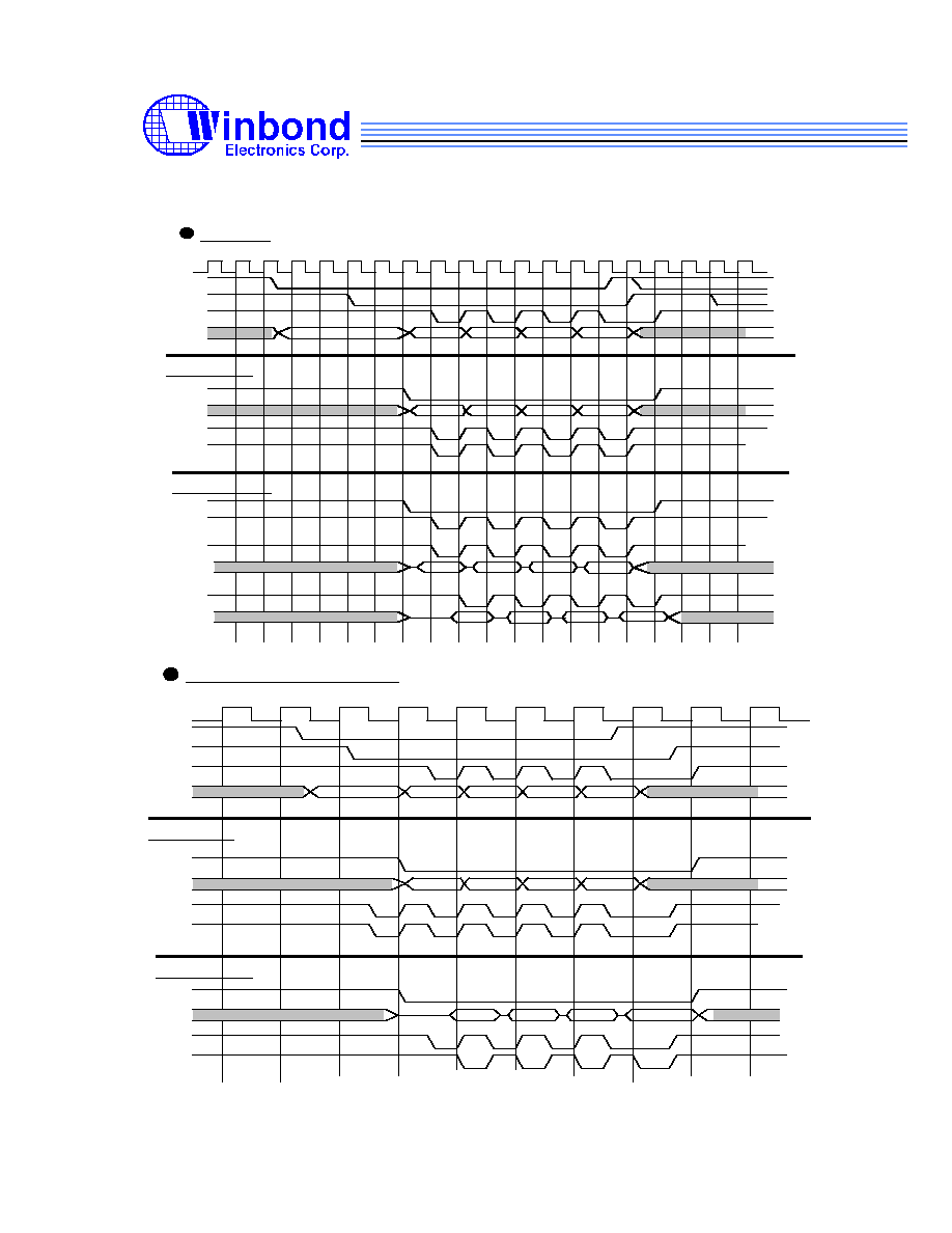
Timing
Normal Case
Data
C
Data
C+1
Data
C+2
Data
C+3
CLK
MCS#
RAS#
CAS#
MD[31:0]
mrdy_
edowr_
WE#
mrdy_
edowr_
OE#
Row Addr.
R
Column
C
Column
C+1
Column
C+2
Column
C+3
ADD[9:0]
Write to DRAM
Read from DRAM
edowr_
Data
C
Data
C+1
Data
C+2
Data
C+3
MD[31:0]
Data
C
Data
C+1
Data
C+2
Data
C+3
MD[31:0]
(Fast mode)
(EDO mode)
At E6F4 Mode (EDO-60, 40MHz )
Row Addr.
R
Column
C
Column
C+1
Column
C+2
Column
C+3
Data
C
Data
C+1
Data
C+2
Data
C+3
Data
C
Data
C+1
Data
C+2
Data
C+3
CLK
MCS#
RAS#
CAS#
ADD[9:0]
MD[31:0]
mrdy_
edowr_
WE#
MD[31:0]
mrdy_
edowr_
OE#
Write to DRAM
Read from DRAM

W9960CF
Winbond Confidential
30
June 1997
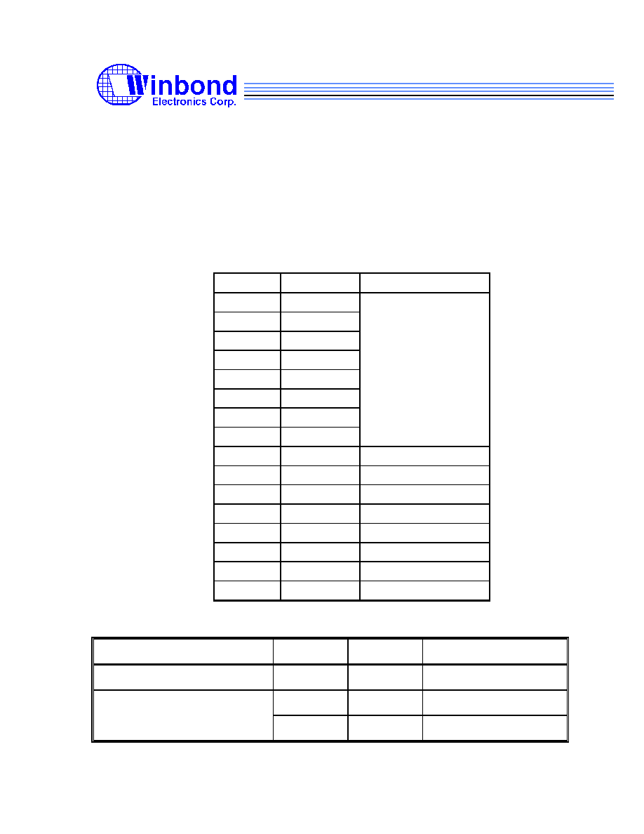
3.7 INTERRUPT/TRIGGER Controller
This controller provides 10 different Interrupts to VRISC and 5 triggering signals for VRISC to
trigger engines.
Trigger #0 is used for Video Capture triggering. Trigger #1 is used to start ME motion estimation
search. Trigger #2 is used to start FILTER block operation. Trigger #3 is used to trigger IDCT to
start decoding inverse discrete cosine transform operation. Trigger #4 is used to trigger DCT to
start encoding forward discrete cosine transform.
Interrupt #5 is XDMA Terminal Count Interrupt. Interrupt #6 is the interrupt coming from ISA-like
external interface. Interrupt #7 indicates the VLE FIFO full while T-coeff. encoding. Interrupt #8
and #9 are TIMER TR (Temporal Reference) Interrupts for decoding and encoding. Interrupt #10
and #11 are the TIMER time out interrupts. Interrupt #12 is used for host to interrupt VRISC.
Interrupt #13 indicates VLD operation is completed after VLD command register is triggered.
Interrupt #14 indicates the PIO BCH code is not aligned with frame. Interrupt #15 indicates a
Run-Level Block Error in VLD decoding.
All interrupts can be enabled or disabled as specified by the mask bits of the IMSK register. It will
response which channel is active on ISR register and generate an INT to VRISC. When VRISC
enters an interrupt service routine, it has to read out the IVEC register to have Interrupt
Controller assert INTA to clear interrupt status.
Signal
Type
INTG_IN
INTG_OUT
ENGINE
Description
0
TRIG
Capture_Trigger
VideoPre
Video Capture trigger
1
TRIG
MERDY
METG
ME
Trigger Motion Estimation
2
TRIG
FRDY
F_TRIGGER
FILTER
Trigger Filter
3
TRIG
TendINT
TriggerDEC
DCT/IDCT
Trigger IDCT
4
TRIG
RISCINT
TriggerENC
DCT/IDCT
Trigger DCT
5
INTR
int1
XDMA
XDMA TC Interrupt
6
INTR
extint
ISA-Like
ISA External Interrupt
7
INTR
VLE_INT
VLETCO
VLE FIFO Full Interrupt
8
INTR
DTR_INT
TIMER
Temp. Ref. Interrupt (Decoder)
9
INTR
ETR_INT
TIMER
Temp. Ref. Interrupt (Encoder)
10
INTR
TOUT0
TIMER
Timer 0 interrupt
11
INTR
TOUT1
TIMER
Timer 1 interrupt
12
INTR
PCI_INT
HOST
Host interrupt RISC
13
INTR
VLRDY_INT
TG_INTA
PIO
VLD is over
14
INTR UFRAME_INT UFRAME_INTA
PIO
Frame Un-lock Interrupt
15
INTR VLDREQ_INT VLDREQ_INTA
VLD
VLD Run Level Block Error

W9960CF
Winbond Confidential
31
June 1997
Block Diagram
IMSK
ISR
Queue
IVEC
INT
STG
TMODE
ITrig
CPU_Bus
Irdy
INTG Registers
RISC Address/PCI Offset Address
Name
Read/Write
Description
0019H/0064H
IMSK
R/W
Interrupt Mask Register
001AH/0068H
ISR
R
Interrupt Status Register
001BH/006CH
IVEC
R/W
Interrupt Vector Register
001CH/0070H
TMOD
R/W
Trigger Mode Register
001DH/0074H
STG
W
Software Trigger Register
W9960CF
Winbond Confidential
32
June 1997
3.8 X_INTERRUPT Controller ( XINTC )
XINTC provides 16 channels interrupt trigger source and generates INTA# to PCI_BUS.
Channel #0~#7 are used for XDMA requests. Channel #8~#11 are reserved for VRISC to issue
interrupts to host. Channel #12 is for the ISA-like external Interrupt. Channel#13~#14 are the TC
interrupts for XDMA and FDMA. Channel#15 is the interrupt from INTC controller. All channels
are maskable by XMSK register. Host has to read the XSTS register to identify interrupt source
when receiving a W9960CF issued interrupt. Host issues interrupt to VRISC by programming
PCI_INT register, which will generate a interrupt trigger pulse for VRISC to enter interrupt service
routine.
Channel
XINT_IN
Description
0
xdreq0
dreq of XDMAC
1
xdreq1
2
xdreq2
3
xdreq3
4
xdreq4
5
xdreq5
6
xdreq6
7
xdreq7
8
1
(Reserved for VRISC)
9
1
(Reserved for VRISC)
10
1
(Reserved for VRISC)
11
1
(Reserved for VRISC)
12
extint
ISA External Interrupt
13
int1
tc of XDMAC
14
tc_out
tc of FDMAC
15
int
INT of INTG
XINTC Registers
RISC Address/PCI Offset Address
Name
Read/Write
Description
0006H/0018H
XMSK
R/W
X_Interrupt Mask Register
0007H/001CH
XSTS
R
X_Status Register
PCI_INT
W
PCI_INT Command
W9960CF
Winbond Confidential
33
June 1997
3.9 GPIO ( General Purpose Input/Ouput) Port
W9960CF provides 4 pins as a GPIO port. These four pins are programmable to be input or
output. GPIO0 and GPIO1 are two open drain IO pads and pull-high resistors are necessary in
application circuits. GPIO2 and GPIO3 are tri-state IO pads. GPIO port is used to connect to
external devices such as analog video decoder and/or audio coprocessor.
wr_(CPU Bus)
rd_(CPU Bus)
GPIO[3:2]
GPIO[1:0]
1
0
0
1
0
0
Hi-Z
Hi-Z
Hi-Z
Hi-Z
Hi-Z
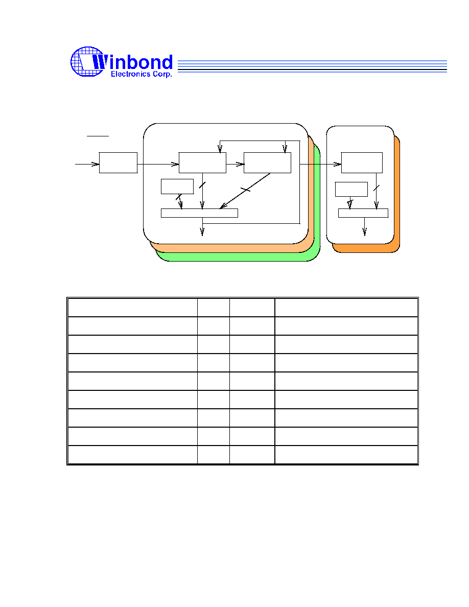
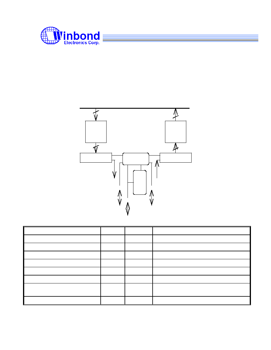
3.10 TIMER
W9960CF provides a programmable pre-scale counter (PSR register) for different Video Clock
input and three period registers (TP0~TP2) for period setting of the temporal reference, time
counter and DRAM reference. W9960 also provides two TR reference counters for decoding and
encoding (DTR and ETR registers). Here is the programming example:
if the video clock (CLK_Video pin) is 13.5MHz, set:
RC2~RC0 to 010b,
P3~P0 to 0011b
TP0= 6DF8h (29.97016frame/sec), 83D5h (25.00 frame/sec),
TP2=000Dh;
If the Video clock is 27MHz, set:
RC2~RC0= 010b,
P3~P0=0100b,
TP0= 6DF8h (29.97016frame/sec), 83D5h (25.00 frame/sec),
TP2=000Dh.
The frequency calculation statement is as:
Fre. = VCLK / ( (2**
(
N+1)
)*(TP+1) )
where VCLK is input frequency of CLK_Video pin, N is the value of RC[2:0], and TP is the
period setting of TP0, TP1, or TP2.
W9960CF
Winbond Confidential
34
June 1997
Block Diagram
TIMER
Pre-Scaler
(/2 ~ /2 )
16
Counter
(8 stages)
Counter
(8 stages)
16
8
8
TP
register
Comparetor
TRV Counter
(8 stages)
TOUT Interrupt
TER
register
Comparetor
8
8
TR_INT
Video
Clock
TIMER Registers
RISC Address / PCI Offset Address
Name
Read/Write
010H / 040H
PSR
R/W
Pre-Scale Register
011H / 044H
TR0
R
Timer Register #0
012H / 048H
TR1
R
Timer Register #1
013H / 04CH
DTR
R/W
Temporal Reference of Decode Register
014H / 050H
TP0
R/W
Timer Period Register #0
015H / 054H
TP1
R/W
Timer Period Register #1
016H / 058H
TP2
R/W
Timer Period Register #2
017H / 05CH
ETR
R/W
Temporal Reference of Encode Register
W9960CF
Winbond Confidential
35
June 1997
3.11 Video Pre/Post Processing Engine
The functions of Video Preprocessing engine are capturing, cropping, zooming video in 4CIF,
CIF, QCIF, Sub-QCIF resolution. Actually, user can command this engine to capture image of
any size within 704 x 576(PAL) or 704x480(NTSC). Video Preprocessing Engine also provides
two programmable decimation horizontal filters for luminance data and chrominance data to
smooth the captured image.
Video Postprocessing Engine supports both RGB 5:6:5 and YUV 4:2:2 for both local and remote
video output. RGB format is for normal VGA card without color space conversion. YUV format is
for those video cards with color space conversion and scaling support.
3.11.1
V
IDEO
P
RE
P
ROCESSOR
(VPRE)
The Video PreProcessor (VPRE) transfers the captured video data to frame buffer DRAM
through horizontal filters, horizontal subsampler and FIFO for DMA data transfer. The size of the
Y FIFO is 44x4 bytes. U FIFO and V FIFO is 22x4 bytes each. The block diagram is shown
below:
Bt/Ph_
Video
Interface
YUV422
signal
from
Video Decoder
HS
VS
VD(15:0)
VCLK
Image
Grabber
Cap_trig
HD
HA
VD
VA
Even
/Odd
ScaleV
(1, 1/2, 1/5 )
YUV
422
v
420
ScaleH
( 1, 1/2, 1/4 )
1/2H
1/2H
Y
U
V
FIFO
FIFO Control
Full
( 1, 3/4, 2/4, 1/4 )
taps filter
D_Bus
44x32bits
22x32bits
22x32bits
Video PreProcess Diagram
The following is the register parameters used to configure for different formats:
NTSC/
PAL
HA
VA
E
O
Scale
H
Scale
V
1/5
O
Picture Size
( H x V )
Format
Description
NTSC
704
240
on
on
1
1
off
704
480
4CIF
704
240
on
on
1/2
1
on
352
288
CIF
4CIF ZO to CIF
352
240
on
on
1
1
on
352
288
CIF
CIF ZI fr 4CIF ,P
352
144
on
off
1/2
1
off
176
144
QCIF
QCIF ZI fr 4CIF, P
704
240
on
on
1/4
1/2
on
176
144
QCIF
4CIF ZO to QCIF
PAL
704
288
on
on
1
1
off
704
576
4CIF

W9960CF
Winbond Confidential
36
June 1997
704
288
on
off
1/2
1
off
352
288
CIF
352
288
on
on
1
1/2
off
352
288
CIF
352
144
on
off
1/2
1
off
176
144
QCIF
704
288
on
off
1/4
1/2
off
176
144
QCIF
3.11.2 V
IDEO
P
OST
P
ROCESSOR
(VPOST)
VPOST provides an option of 1/2 scaling-down for both local and remote picture. It also supports
color space conversion for either YUV422 or RGB565 video output. VPOST provides FIFO for
DMA data transfer. The size of Y FIFO is 16x4bytes. U
FIFO and V FIFO is 8x4 bytes each.
deci2y
deci2u
deci2v
BUFFER
Y
U
V
deci2
Trig
16x4bytes
8x4bytes
8x4bytes
Colour
Space
Convert
YUV422 -> RGB565
rgb
D_Bus
PACK
X_Bus
Vout
Video PostProcessor Diagram
W9960CF
Winbond Confidential
37
June 1997
VIDEO Register
RISC Address/PCI Offset Address
Name
Read/Write
Description
01A0H/0680H
VPRE Mode
R/W
Video Preprocessing operation mode
01A1H/0684H
HDelay
R/W
Horizontal delay pixel number
01A2H/0688H
VDelay
R/W
Vertical delay line number
01A3H/068CH
HA
R/W
Horizontal active pixel number
01A4H/0690H
VA
R/W
Vertical active line number
015AH/0694H
LFP
R/W
Luminance filter parameters, Tap1 and
Tap2
01A6H/0698H
CFP
R/W
Chrominance filter parameters, Tap1
and Tap2.Luminance decimation filter
parameter Tap3.
01A7H/069CH
VPOST Mode
R/W
VideoPostprocessor operation mode
W9960CF
Winbond Confidential
38
June 1997
3.12 Motion Estimation Engine
W9960CF motion estimation (ME) engine implements full search matching algorithm (FSA),
which is widely used thanks to its simplicity and regularity. In this algorithm, for each reference
block in the current frame, the previous frame is searched within a neighborhood, i.e. search
window, to find the most matched pixel block.
CONTROL
LOGIC
Caddr
Saddr
MV
MAD,MA,MB,MX
Comparator
8*PE
8*PE
p'
ph
ph'
p
c
1.5
Search
window
Current
block
DMA-data
DMA-addr
DMA-request
DMA-ack
INT-request
Trigger
CPU-bus
half-pixel
Search
Window
Half-Pixel
Accelerator
Mode
SREGION
Half-Pixel
ME Registers
RISC Address/PCI Offset Address
Name
Read/Write
Description
0190H / 0640H
MEMODE
R/W
Mode Register
0191H / 0644H
MVR
R/W
Motion Vector Register
0192H / 0648H
MADR
R/W
Mean Absolute Difference Register
0193H / 064CH
MBR
R/W
Mean Current Macro Block Register
0194H / 0650H
MAR
R/W
Mean Average Difference Register
0195H / 0654H
MXR
R/W
Mean First Search Register
0196H / 0658H
SRGION
R/W
Search Region Register

W9960CF
Winbond Confidential
39
June 1997
3.13 FILTER Engine
Filter Engine implements the loop filter function of H.261. It is a two-dimensional spatial filter as
shown below. The Filter Engine also performs the interpolation function of half pixel prediction
and PB frame prediction in H.263.
H.261 8x8 predicted Block with 1-2-1 Filter
0
1
2
3
4
5
6
7
1 2 1
8
9
10
11
12
13
14
15
(1) 1/16
2 4 2
for pixels inside the block
16
17
18
19
20
21
22
23
1 2 1
24
25
26
27
28
29
30
31
32
33
34
35
36
37
38
39
(2) 1/16 | 4 8 4 | for pixels on the block edge
40
41
42
43
44
45
46
47
48
49
50
51
52
53
54
55
(3) 1/16 | 16 | for pixels on the block corner positions
56
57
58
59
60
61
62
63

W9960CF
Winbond Confidential
40
June 1997
H.261 1-2-1 Filter Table
1
1 2 1
1 2 1
1 2 1
1 2 1
1 2 1
1 2 1
1
1
2
1
1 2 1
2 4 2
1 2 1
1 2 1
2 4 2
1 2 1
1 2 1
2 4 2
1 2 1
1 2 1
2 4 2
1 2 1
1 2 1
2 4 2
1 2 1
1 2 1
2 4 2
1 2 1
1
2
1
1
2
1
1 2 1
2 4 2
1 2 1
1 2 1
2 4 2
1 2 1
1 2 1
2 4 2
1 2 1
1 2 1
2 4 2
1 2 1
1 2 1
2 4 2
1 2 1
1 2 1
2 4 2
1 2 1
1
2
1
1
2
1
1 2 1
2 4 2
1 2 1
1 2 1
2 4 2
1 2 1
1 2 1
2 4 2
1 2 1
1 2 1
2 4 2
1 2 1
1 2 1
2 4 2
1 2 1
1 2 1
2 4 2
1 2 1
1
2
1
1
2
1
1 2 1
2 4 2
1 2 1
1 2 1
2 4 2
1 2 1
1 2 1
2 4 2
1 2 1
1 2 1
2 4 2
1 2 1
1 2 1
2 4 2
1 2 1
1 2 1
2 4 2
1 2 1
1
2
1
1
2
1
1 2 1
2 4 2
1 2 1
1 2 1
2 4 2
1 2 1
1 2 1
2 4 2
1 2 1
1 2 1
2 4 2
1 2 1
1 2 1
2 4 2
1 2 1
1 2 1
2 4 2
1 2 1
1
2
1
1
2
1
1 2 1
2 4 2
1 2 1
1 2 1
2 4 2
1 2 1
1 2 1
2 4 2
1 2 1
1 2 1
2 4 2
1 2 1
1 2 1
2 4 2
1 2 1
1 2 1
2 4 2
1 2 1
1
2
1
1
1 2 1
1 2 1
1 2 1
1 2 1
1 2 1
1 2 1
1
Block Diagram
The prediction picture is transferred into Filter Engine by DMA operation. Half Pixel
PreProcessor module performs the half pixel interpolation in x-axial direction. HPP module
performs the half pixel interpolation in y-axial direction. OMC module performs PB frame
prediction. The control flow is specified in FCR0 (Filter Control Register #0) and BRR (Bi-
direction Range Register) registers.

W9960CF
Winbond Confidential
41
June 1997
dmablk
9
8
MUX
MUX
0
8
8
1
8
8
2
8
8
F/F
F/F
MUX
F/F
F/F
0,1,2/8,4/8
4/8,8/8,4/8,8/8
0,1,2/8
CSA
ADDER
F/F
F/F
0,1/4, 2/4
0,2/4,4/4
0,1/4
CSA
ADDER
F/F
Input from DRAM Controller
To DCT/IDCT Engine
or DRAM Controller
Half Pixel
PreProcessor
F/F
HPP
OMC
dctblk
8
8
Filter Registers
RISC Address / PCI Offset Address
Name
Read/Write
018CH / 0630H
FCR0
R/W
Filter Control Register #0
018DH / 0634H
FCR1
R/W
Filter Control Register #1
018EH / 0638H
BRR
R/W
Bi-direction Range Register
W9960CF
Winbond Confidential
42
June 1997
3.14 FIDCT/Q/IQ Engine
W9960CF contains Forward/Inverse Discrete Cosine Transform Engine (FIDCT) and
Quantization /Inverse Quantization Engine, which are frequently used in video
compression/decompression.
For video encoding, DCT is used to reduce spatial redundancy of images. The quantization logic
further filters most AC values and keeps the DC value.
In video decoding, each 8x8 block is transformed back by Inverse Quantization. This IQ process
induces quantization error in AC values compared with original data, but the DC value is
recovered losslessly. Thereafter, data is sent to Inverse Discrete Cosine Transform stage to do
image recovery process. In the INTRA mode, the result is final reconstructed image. While in
the INTER mode, the result has to be added with the previous block data to reconstruct the
image.
Block Diagram
ADD
DCT
Q
Zig/Zag
IQ
IDCT
ADD
Quant
Table
From VLD
From Filter
BUFFER
BUFFER
BUFFER
RE-Construct
Current Block
W9960CF
Winbond Confidential
43
June 1997
DCT/IDCT Register
RISC address/PCI Offset Address
Name
Read/Write Description
0180H/0600H
Q_Control
R/W
Quantization value selection
0182H/0608H
CBP threshold
R/W
CBP threshold value
0183H/060CH
CheckSum
R/W
DCT result checksum
0184H/0610H
EQuant value
R/W
Encoding loop Quant value
0185H/0614H
DQuant value
R/W
Decoding loop Quant value
0186H/0618H
EBD Quant value
R/W
Encoding loop BQ/DQ value
0187H/061CH
DBD Quant value
R/W
Decoding loop BQ/DQ value
0188H/0620H
CODEC
R/W
Intra/inter mode, coding/decoding

W9960CF
Winbond Confidential
44
June 1997
3.15 Programmable Input/Output Engine
Programmable input/output (PIO) engine can control the input bit stream data from X_bus or
CPU_data_bus to the variable length decoder (VLD). PIO plays the role of interface between the
frame memory (FM) and X_bus during bitstream receiving for decoding and bitstream
transmission after encoding.
Block Diagram
FM-R
FM-T
VLD
CR1
CR2
CT1
CR3
CT2
P<S
BCH
ENCODER
BCH
DECODER
P>S
S>P
S<P
1
1
1
1
1
BCH
DECODE
FIFO
OUTPUT
DATA
FIFO
INPUT
DATA
FIFO
ENCODE
FIFO
DECODER
FIFO
DREQ
DECF
XDREQ_IPTF
DREQ
ENCF
XDREQ_OPTF
CPU
BUS
X_BUS
W9960CF
Winbond Confidential
45
June 1997
PIO Registers
RISC Address/PCI Offset Address
Name
Read/Write
Description
01A8H / 06A0H
CDFIFO_H
R/W
Compressed Data FIFO High Word Register
01A9H / 06A4H
CDFIFO_L
R/W
Compressed Data FIFO Low Word Register
01AAH / 06A8H
PIOCTL
R/W
PIO Control Register
01ABH / 06ACH
XDMAR
R/W
X_Bus DMA Request Enable Register
01ACH / 06B0H
FDMAR
R/W
Frame Memory DMA Request Enable Register
01ADH / 06B4H
FC
R/W
Frame Code Register
01AEH / 06B8H
LPD
R/W
Lock Position Detect Register
01AFH / 06BCH
IOFSR
R/W
Input/Output FIFO Status Register
W9960CF
Winbond Confidential
46
June 1997
3.16 Variable Length Code Decoder
The Variable Length (VL) Engine uses the code books or lookup tables to map the Huffman code
words. Huffman coding is a kind of entropy coding method used in H26X. Image or video data
size can be reduced significantly when proper Huffman tables are used. Not only the variable
length codes but also the fixed length codes can be decoded in this engine
.
Bit streams coming
from the programmable in/out port (PIO) are fed into VL engine during decoding process.
VLD Register
RISC Address / PCI Offset Address
Name
Read/Write
Description
01B8H / 06E0H
MCR_L
R/W
Match Code Low Word Register
01B9H / 06E4H
MCR_H
R/W
Match Code High Word Register
01BAH / 06E8H
MSR
R/W
Match Size Register
01BBH / 06ECH
VLCMD
R/W
VL Command Register
01BCH / 06F0H
VLRES
R
VL Result Register
01BDH / 06F4H
VLRES_LW
R
VL Result Low Word Register
RISC Address / PCI Offset Address
Name
Read/Write
Description
01C0H / 0700H
VLDTC0
R/W
VLD TCoefficient Register 0
................
..................
.......
...................................................
01FFH / 07FCH
VLDTC63
R/W
VLD Tcoefficient Register 63
W9960CF
Winbond Confidential
47
June 1997
3.17 Audio Coprocessor Interface
W9960CF provides an ADSP-21xx SPORT compatible serial port to interface to audio
coprocessors. Multi-channel mode in AD SPORT0 is provided for interfacing with other chips
time-division multiplexing (TDM) function. Transmitter FIFO and Receiver FIFO are used since
serial one-bit bit stream is packed into 32-bit word, and no CPU instructions to access Tx or Rx
registers. This T/R FIFO should access with frame memory via 32-bit X_bus. No compounding
function is provided with, since no management for u-law or A-law data format.
Block Diagram
TFS
RFS
DT
DR
Tx
Rx
ISCLK
Serial
Control
Transmit
Shift Reg
Receive
Shift Reg
SCLK
32
32
16
16
X_BUS
AUDIO PORT Register
RISC Address / PCI Offset Address
Name
Read/Write
Description
0198H / 0660H
ACTL
R/W
Audio Port Control Register
0199H / 0664H
SCLKDIV
R/W
Serial Clock Divisor Register
019AH / 0668H
RFSDIV
R/W
Receive Frame Sync Divisor Register
019BH / 066CH
RWE_L
R/W
Receive Word Enables for Low Word Register
019CH / 0670H
RWE_H
R/W
Receive Word Enables for High Word Register
019DH / 0674H
TWE_L
R/W
Transmit Word Enables for Low Word Register
019EH / 0678H
TWE_H
R/W
Transmit Word Enables for High Word
Register
019FH / 067CH
TRBDR
R
Transmit/Receive Buffer Detect Register
W9960CF
Winbond Confidential
48
June 1997
3.18 Variable Length Code Encoding (VLE) Engine
There are two modules in VLE Engine, one is for Tcoeff (Transform coefficient) encoding and the
other is for variable length encoding. The Tcoeff is based on the run level pair generated from
the result of DCT/Quantization and pushed into the 16x32-bit Tcoeff_FIFO. When DCT/Q is
completed, VRISC shall check some conditions such as checksum register and determine
whether to trigger RLC ( Run Level Code ) to generate transform coefficient. When all blocks is
encoded into Tcoeff_FIFO, VRISC shall read Bit Length Register to check how many bits are
generated (overflow condition if Bit Length Register is over 512, busy condition if Bit Length
Register is Zero). Then VRISC read out the Tcoeff value from Tcoeff Result Register. VLE_INT
will assert when the coding bit length is over the threshold of Tcoff_FIFO. VRISC can also write a
command including data and table-indicator into Command Register to generate variable length
code ( except Tcoeff ).
Block Diagram
DCT/QUANT
RLC
Tcoeff-VLE
16 x 32bit
FIFO
DCT_Trig
DCT_rdy
VLE_INT
( Tcoeff FIFO overflow )
RLC_Trig
Tcoeff Result Register
Bit Length Register
VLE Command Register
VLC Table
VLE Result Register
INTRA/
INTER
H261/H263/MPEG/JPEG
VLE Register
RISC Address/PCI Offset Address
Name
Read/Write
Description
01B4H / 06D0H
BLR
R
Bit Length Register
01B5H / 06D4H
TRR
R
Tcoeff Result Register
01B6H / 06D8H
VRR
R
VLE Result Register
01B7H / 06DCH
VCR
W
VLE Command Register
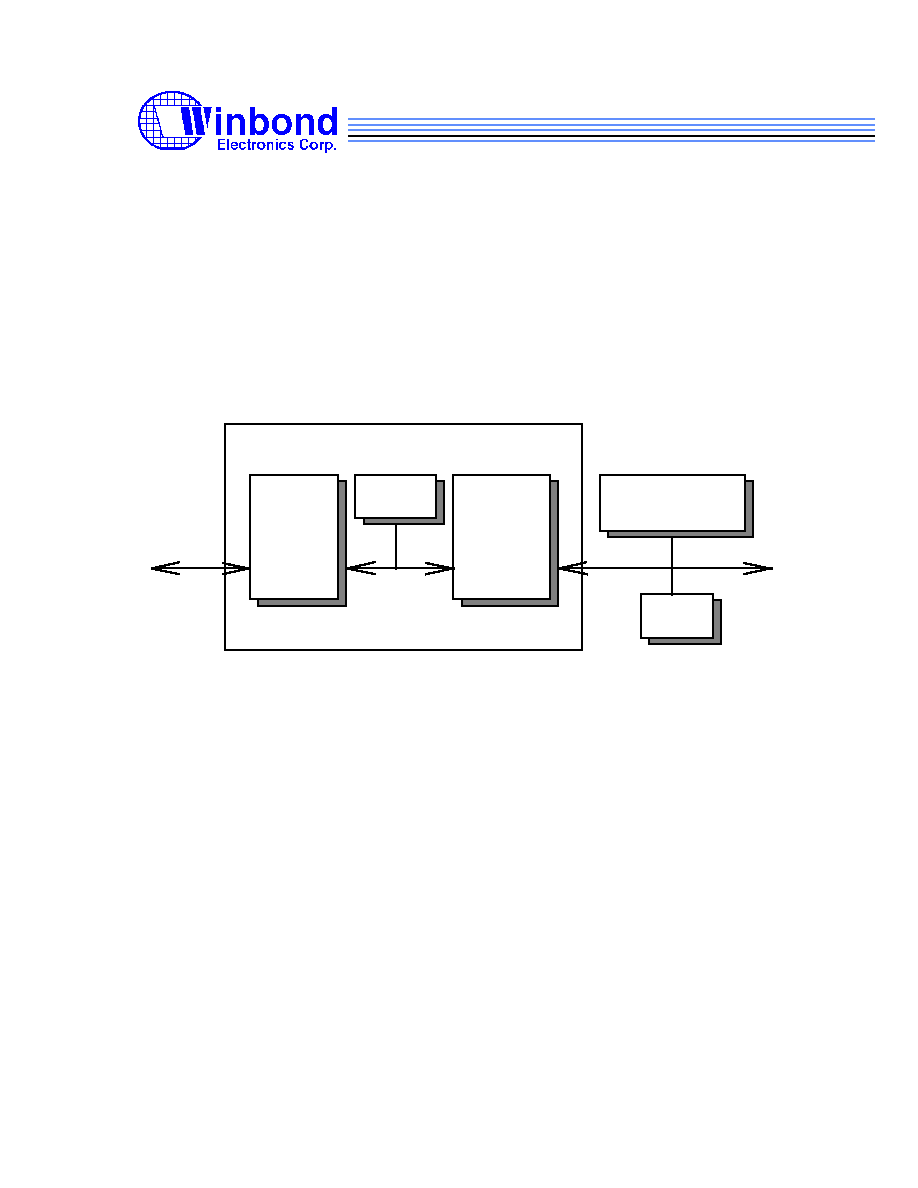
W9960CF
Winbond Confidential 49 June 1997
3.19 ISA-like Interface
The ISA-like Interface implements a parallel I/O port to connect to co-processors, and a Boot-
ROM mechanism to download VRISC firmware automatically.
This ISA-like parallel I/O port provides an 8-bit data bus and 16-bit address bus to connect to co-
processor easily. The host can access the connected co-processor through W9960CF PCI
interface and this ISA-like interface. In this sense, W9960CF acts as a PCI to ISA bridge. It also
provides two external interrupt requests of level or edge trigger.
This ISA-like Interface provides another path to download VRISC firmware in addition to the PCI-
bus interface. In Boot-ROM mode, the ISA-like interface will issue Boot-ROM access cycle to
download firmware after W9960CF is reset.
I S A - L i k e
I n t e r f a c e
R I S C
P C I
I n t e r f a c e
I n t e r n a l B u s
P C I B u s
W 9 9 6 0 C F
C o - P r o c e s s o r
R O M

W9960CF
Winbond Confidential 50 June 1997
ISA-Like Interface Resigisters
RISC Address/PCI Offset Address Name Read/Write Description
020H/080H ISACTL R/W
Setting ISA control operation register
021H/084H SAADDR R/W
Setting ISA output address register
022H/088H SADATA R/W
ISA input/output data register
023H/08CH ISAINT R/W
External interrupt control/status register
Programming Sequence
W9960CF assert I/O read/write cycles on ISA-like interface accroding to the following
programming sequence.
Store ISACTL register
(set WE bit enable)
Store ISAADDR register
(set effective address)
Store ISADATA register
(set effective data)
Store ISACTL register
(set RE bit enable)
Store ISAADDR register
(set effective address)
Load ISADATA register
(read effective data)
Insert Delay
(7-14 clock cycles)
IO Write Cycle IO Read Cycle

W9960CF
Winbond Confidential
51
June 1997
4. W9960CF REGISTERS
4.1 PCI Configuration Registers
Address \ Bit
31 24
23 16
15 8
7 0
00H
Device ID
Vendor ID
04H
Status
Command
08H
Class Code
Revision ID
0CH
Reserved
Header Type
Latency Timer
Reserved
10H
Base Address Register 0 (BAR0)
14H
Base Address Register 1 (BAR1)
18H - 38H
Reserved
3CH
Reserved
Reserved
Interrupt Pin
Interrupt Line
Device/Vendor ID Register
Read-only
PCI Configuration Address: 00H
Default: 9960 1050H
31
30
29
28
27
26
25
24
23
22
21
20
19
18
17
16
Device ID
15
14
13
12
11
10
9
8
7
6
5
4
3
2
1
0
Vendor ID
Bits 31-16 Device ID
Device ID allocated for the W9960 is 9960H.
Bits 15-0
Vendor ID
Vendor ID is allocated by the PCI SIG to ensure uniqueness. The value assigned to
Winbond Electronic Corp. is 1050H.
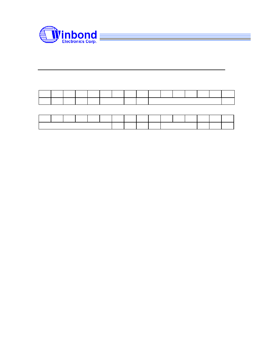
W9960CF
Winbond Confidential
52
June 1997
Status/Command Register
Read/Write
PCI Configuration Address: 04H
Default: 0280 0000H
31
30
29
28
27
26
25
24
23
22
21
20
19
18
17
16
DPE SSE
RMA RTA
STA
DEVSEL
MDP FBC
Reserved
CLK
15
14
13
12
11
10
9
8
7
6
5
4
3
2
1
0
Reserved
FBE
SEE
-
PEE
Reserved
BME MSE -
Bit 31
DPE ( this bit will be clear to 0 , if the write data in the corresponding bit location is a 1 )
Detected Parity Error
1 = Parity Error
0 = Parity Correct
Bit 30
SSE ( this bit will be clear to 0 , if the write data in the corresponding bit location is a 1 )
Signaled System Error
1 = System Error
0 = System Correct
Bit 29
RMA ( this bit will be clear to 0 , if the write data in the corresponding bit location is a 1 )
Received Master Abort
1 = Master Abort On
0 = Off
Bit 28
RTA ( this bit will be clear to 0 , if the write data in the corresponding bit location is a 1 )
Received Target Abort
1 = Target Abort On
0 = Off
Bit 27
STA ( this bit will be clear to 0 , if the write data in the corresponding bit location is a 1 )
Signaled Target Abort
1 = Target Abort On
0 = Off
Bits 26-25 DEVSEL Timing ( Read only )

W9960CF
Winbond Confidential
53
June 1997
01 = Medium DEVSEL# timing
Bit 24
MDP ( this bit will be clear to 0 , if the write data in the corresponding bit location is a 1 )
Master Data Parity Error Detected
1 = Detect Parity Error
0 = Parity Correct
Bit 23
FBC
Fast Back-to-Back Capable ( Read only )
1 = Support Fast Back-to-Back Capable
Bits 22-17 Reserved
Bit 16
CLK
PCI CLK Support ( Read only )
0 = 33Mhz
Bits 15-10 Reserved
Bit 9
FBE
Fast Back-to-Back Enable
1 = Enable
0 = Disable
Bit 8
SERR# Enable
1 = Enable
0 = Disable
Bit 7
Reserved
Bit 6
PEE
Parity Error Response Enable
1 = Enable
0 = Disable
Bits 5-3
Reserved
Bit 2
BME : Bus Master Enable
1 = Enable
0 = Disable
Bit 1
MSE
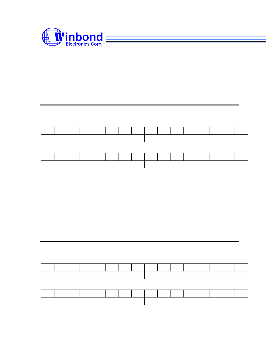
W9960CF
Winbond Confidential
54
June 1997
Memory Space Enable
1 = Enable the device response to memory space accesses
0 = Disable the device response to memory space accesses
Bit 0
Reserved
Class Code/Revision ID Register
Read-only
PCI Configuration Address: 08H
Default: 0400 0000H
31
30
29
28
27
26
25
24
23
22
21
20
19
18
17
16
Base Class Code
Sub-Class Code
15
14
13
12
11
10
9
8
7
6
5
4
3
2
1
0
Programming Interface
Revision ID
Bits 31-24 Base Class Code
Bits 23-16 Sub-Class Code
Bits 15-8
Programming Interface
Bits 7-0
Revision ID
Bits 31-8 are hardwired to 040000H to specify that the W9960 is a multimedia device.
Header Type / Latency Timer Register
Read-Write
PCI Configuration Address: 0CH
Default: 0000 FF00H
31
30
29
28
27
26
25
24
23
22
21
20
19
18
17
16
Reserved
Header Type
15
14
13
12
11
10
9
8
7
6
5
4
3
2
1
0
Latency Timer
Reserved
W9960CF
Winbond Confidential
55
June 1997
Bits 31-24 Reserved
Bits 23-16 Header Type ( Read only )
00H = Type 00H
Bits 15-8
Latency Timer for Master
the low-order 3 bits are read only, high-order 5 bits are read-writable
Bits 7-0
Reserved
Base Address 0 Register
Read/Write
PCI Configuration Address: 10H
Default: 0000 0000H
31
30
29
28
27
26
25
24
23
22
21
20
19
18
17
16
Base Address 0
15
14
13
12
11
10
9
8
7
6
5
4
3
2
1
0
Base Address 0
Bits 31-0
Base Address 0
This field can be used to relocate memory address space to any location that is aligned to
4 Kbytes for mapping W9960 Engine Registers and Data Memory.
The low-order 12bits are read only and hardwired to 000H, the high-order 20bits are read-
writable.
Base Address 1 Register
Read/Write
PCI Configuration Address: 14H
Default: 0000 0000H
31
30
29
28
27
26
25
24
23
22
21
20
19
18
17
16
Base Address 1
15
14
13
12
11
10
9
8
7
6
5
4
3
2
1
0

W9960CF
Winbond Confidential
56
June 1997
Base Address 1
Bits 31-0
Base Address 1
This field can be used to relocate memory address space to any location that is aligned to
4 Mbytes for mapping W9960 DRAM Frame Memory. The low-order 22bits are read only
and hardwired to 0_0000H, the high-order 10bits are read-writable.
Interrupt Line Register
Read/Write
PCI Configuration Address: 3CH
Default: 00H
7
6
5
4
3
2
1
0
Interrupt Line
Bits 7-0
Interrupt Line
This 8-bit register is used to communicate interrupt line routing information. POST software
will write the routing information into this register as it initializes and configures the system.
Interrupt Pin Register
Read-only
PCI Configuration Address: 3DH
Default: 01H
7
6
5
4
3
2
1
0
Interrupt Pin
Bits 7-0
Interrupt Line (hardwired to 01H)
This register is hardwired to 1 to specify that INTA# is the interrupt pin used.
W9960CF
Winbond Confidential
57
June 1997
5. ELECTRICAL SPECIFICATIONS
5.1 Absolute Maximum Ratings
Ambient temperature
0
o
C to 70
o
C
Storage temperature
-40
o
C to 125
o
C
DC supply voltage
-0.5V to 5V
I/O pin voltage with respect to Vss
-0.5V to VDD+0.5V
5.2 DC Specifications
(V
DD
= 3.0V to 3.6V, V
SS
= 0V, V
DD5V
= 5V, TA=0
o
C to 70
o
C)
Symbol
Parameter
Min
Typ
Max
Unit
Conditions
V
IL
Input Low Voltage
0.8
V
V
IH
Input High Voltage
2.0
V
V
OL
Output Low Voltage
Vss+0.4
V
I
OL
=10mA
V
OH
Output High Voltage
2.4
V
I
OH
=6mA
I
IL
Input Low Current
�
10
�
A
I
IH
Input High Current
�
10
�
A
I
OZ
Output Tri-state Current
�
10
�
A
C
IN
Input Capacitance
10
pF
C
OUT
Output Capacitance
50
pF
I
CC
Power Supply Current
400
mA
5.3 AC Specifications

W9960CF
Winbond Confidential
58
June 1997
5.3.1
C
LOCK
S
PECIFICATION
0.6VDD
0.5VDD
0.4VDD
0.3VDD
t
cyc
high
low
t
t
3.3 Volt Clock
0.2VDD
Symbol
Parameter
Min
Max
Units
t
cyc
CLK Cycle Time
30
ns
t
high
CLK High Time
11
ns
t
low
CLK Low Time
11
ns
CLK Slew Rate
1
4
V/ns
5.3.2
R
ESET
T
IMING
RST
#
t
Lo
w
Symbol
Parameter
Min
Max
Unit
t
Low
System reset active pulse width
10
t
cyc
ns
W9960CF
Winbond Confidential
59
June 1997
5.3.3
PCI I
NTERFACE
AC T
IMING
C L K
O U T P U T
D E L A Y
Tri_State
O U T P U T
C L K
INPUT
t
val
t
t
t
t
on
off
0.4VDD
0.285VDD (rising edge)
0.615VDD (falling edge)
su
h
inputs
valid
0.4VDD
0.6VDD
0.2VDD
0.4VDD
0.6VDD
0.2VDD
Symbol
Parameter
Min
Max Units
Notes
t
val
CLK to Signal Valid Delay - bused signals
2
11
ns
1
t
val
(ptp)
CLK to Signal Valid Delay - point to point
2
12
ns
2
t
on
Float to Active Delay
2
ns
1,4
t
off
Active to Float Delay
28
ns
1,4
t
su
Input Set Up Time to CLK - bused signals
7
ns
1,3
t
su
(ptp)
Input Set Up Time to CLK - point to point
10
ns
2
t
h
Input Hold Time from CLK
0
ns
1,2,3
Note 1: bused signals : AD31-AD0, C/BE3-C/BE0, PAR, FRAME#, TRDY#, IRDY#, STOP#,
DEVSEL#, PERR#,
Note 2: point to point signals : REQ# is output signal, GNT# is input signal
Note 3: Input Signal : IDSEL
Note 4 : Output Signal : INTA#, SERR#

W9960CF
Winbond Confidential
60
June 1997
5.3.4
AUDIO I
NTERFACE
AC T
IMING
RFS (out)
TFS (out)
DT
SCLK
DR
RFS (in)
TFS (in)
fsd
t
t
scdv
tdv
0.285VDD (rising edge)
0.615VDD (falling edge)
0.4VDD
0.6VDD
0.2VDD
t
t
scs
sch
inputs
valid
0.4VDD
t
t
TFS (in)
sck
Symbol
Parameter
Min
Max
Unit
t
sck
SCLK Period
100
-
ns
t
scs
DR/TFS/RFS Setup Time
Ref. to SCLK falling
10
-
ns
t
sch
DR/TFS/RFS Hold Time
Ref. to SCLK falling
10
-
ns
t
fsd
TFS/RFS Valid Delay from SCLK rising
-
25
ns
t
scdv
DT Valid Delay from SCLK rising
-
25
ns
t
tdv
DT Valid Delay from TFS
(Alternate Frame Mode)
-
20
ns
W9960CF
Winbond Confidential
61
June 1997
5.3.5
DRAM I
NTERFACE
AC T
IMING
CLK_MEM
RAS0#,RAS1#
CAS0#,CAS1#
MA7-MA0
WE1#,WE0#
MD31-MD0
(output)
OE1#,OE0#
MD31-MD0
(input)
Row Addr
Column Addr
Column Addr
Data
Data
t
t
t
t
t
t
t
rv1
rv2
cv1
cv2
t
av
wv
dv
ov
Data
Data
t
t
dsu
dh
Symbol
Parameter
Min
Max
Unit
t
rv1
RAS# valid delay ref. to CLK_MEM rising
14
ns
t
rv2
RAS# valid delay ref. to CLK_MEM falling
14
ns
t
cv1
CAS# valid delay ref. to CLK_MEM falling
12
ns
t
cv2
CAS# valid delay ref. to CLK_MEM rising
16
ns
t
av
Memory address valid delay
20
ns
t
wv
Memory WE# valid delay
14
ns
t
dv
Memory Data valid delay
20
ns
t
ov
Memory OE# valid delay
12
ns
t
dsu
Memory Data setup time
12
ns
t
dh
Memory Data hold time
2
ns
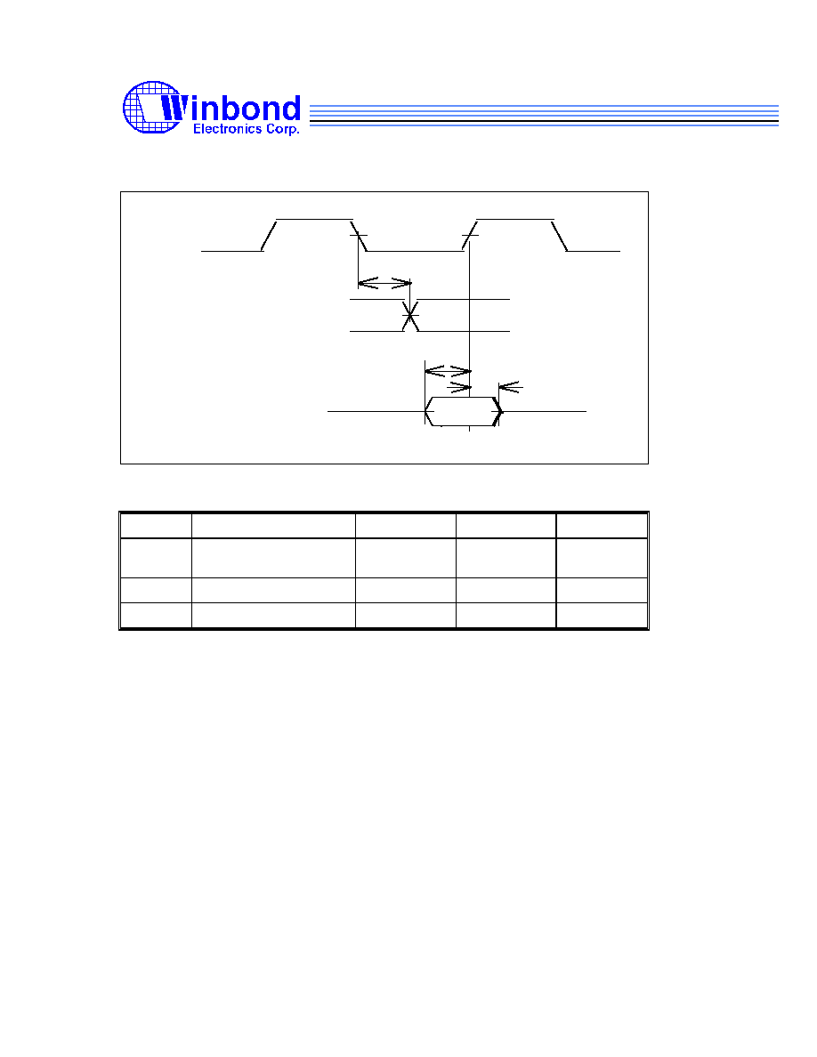
W9960CF
Winbond Confidential
62
June 1997
5.3.6
GPIO AC T
IMING
CLK_MEM
AC
GPIO3-GPIO0
(Output)
SETUP
HOLD
GPIO3-GPIO0
(Input)
t
t
t
Symbol
Parameter
Min
Max
Unit
t
AC
GPIO output access
time
15
ns
t
SETUP
GPIO input set up time
10
ns
t
HOLD
GPIO input hold time
5
ns

W9960CF
Winbond Confidential
63
June 1997
5.3.7 V
IDEO
P
RE
P
ROCESSOR
AC T
IMING
SETUP
HOLD
LLC
LLCL
LLCH
CLK_Video
HREF, VS, HS, VD[15:0]
t
t
t
t
t
Symbol
Parameter
Min
Typ
Max
Unit
t
LLC
CLK_Video period
74
ns
t
LLCL
CLK_Video Low width
37
ns
t
LLCH
CLK_Video High width
37
ns
t
SETUP
Input Set Up time
15
ns
t
HOLD
Input Hold Time
5
ns

W9960CF
Winbond Confidential
64
June 1997
5.3.8
ISA-L
IKE
B
US
AC T
IMING
SAIOW#
SAADDR15-0
SADATA7-0
50ns
150ns
80ns
Address
Data
Waveform of IO Write Operation
SAIOR#
SAADDR15-0
SADATA7-0
Address
Data
Waveform of IO Read Operation
0ns
20ns
150ns
50ns

W9960CF
Winbond Confidential
65
June 1997
6. APPENDIXES
6.1 Porting Guide for W9960 Win95 Device Driver
6.2 Firmware Loading Precedure
6.3 Application/Firmware Command Block