Document Outline
- WM8181
- 12-bit 2MSPS Serial Output CIS/CCD Digitiser
- Advanced Information, January 2000, Rev 3.0
- DESCRIPTION
- FEATURES
- APPLICATIONS
- BLOCK DIAGRAM
- PIN CONFIGURATION
- ORDERING INFORMATION
- PIN DESCRIPTION
- POSSIBLE POWER SUPPLY COMBINATIONS
- ABSOLUTE MAXIMUM RATINGS
- RECOMMENDED OPERATING CONDITIONS
- ELECTRICAL CHARACTERISTICS
- DEVICE DESCRIPTION
- INTRODUCTION
- GENERAL OPERATION
- OVERALL TIMING
- OPERATIONAL TIMING DIAGRAMS
- APPLICATIONS RECOMMENDATIONS
- INTRODUCTION
- PCB LAYOUT
- TYPICAL APPLICATIONS
- CIS SCANNER
- CCD SCANNER
- ADJUSTING THE ADC INPUT RANGE
- RECOMMENDED EXTERNAL COMPONENTS
- PACKAGE DIMENSIONS

WM8181
12-bit 2MSPS Serial Output CIS/CCD Digitiser
Advanced Information, January 2000, Rev 3.0
WOLFSON MICROELECTRONICS LTD
Lutton Court, Bernard Terrace, Edinburgh, EH8 9NX, UK
Tel: +44 (0) 131 667 9386
Fax: +44 (0) 131 667 5176
Email: sales@wolfson.co.uk
http://www.wolfson.co.uk
Advanced Information data sheets contain
preliminary data on new products in the
preproduction phase of development.
Supplementary data will be published at a
later date.
2000 Wolfson Microelectronics Ltd
.
DESCRIPTION
The WM8181 is a 12-bit resolution, 2MSPS single channel
image digitiser which is designed for easy interface to either
CIS or CCD linear image sensors. Data is output in serial
mode. The applied clock frequency (MCLK) equals the bit
rate of the data output. The sample rate of the WM8181 can
be either 1/12th or 1/16th of the applied master clock
frequency.
The device can be configured for either single-ended or
differential input operation. In single ended input mode, a
reset clamp voltage can be applied to the analogue signal,
under the control of a digital signal at the CLAMP pin. The
WM8181 will accept either positive or negative-going video
signals at any voltage between AGND and AVDD. The ADC
references are internally generated. The range of these
references may be derived internally using a bandgap
generator or externally using the VREFIN pin.
The WM8181 is powered from either 3.3V or 5V single
supplies. The device may also be powered from split 5V
and 3.3V dual supplies. Typically, the WM8181 consumes
23mA supply current in normal operation. When the device
is powered down, the supply current falls to less than 1
�
A.
The WM8181 is available in a 16-pin wide-body SOIC
package.
FEATURES
�
12-bit 2MSPS ADC
�
No missing codes
�
Serial output
�
Simple clocking
�
Internal or external ADC reference range control
�
Accepts positive or negative video
�
Rail to rail input range
�
Reset-level clamp switch
�
3.3V or 5V single supplies
�
5V/3.3V dual supplies
�
23mA supply current
�
16-pin wide body SOIC package
APPLICATIONS
�
USB bus powered scanners
�
Flatbed scanners
�
Sheetfeed scanners
�
Contact image sensors (CIS)
�
Linear CCDs
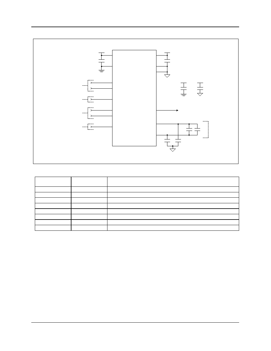
BLOCK DIAGRAM
C L A M P ( 1 1 )
V R E F I N ( 3 )
VINM (5)
VINP (4)
0 . 8 * V D D
(1)
A G N D 1
1 . 5 V
B A N D -
G A P
H O L D
S A M P L E /
(7)
V R T
G E N E R A T O R
V R T / V R B
P D
(2)
A G N D 2
(6)
V R B
1 2
T I M I N G A N D
P O W E R D O W N C O N T R O L
P A R A L L E L
T O
S E R I A L
( 1 0 ) D G N D
( 1 4 ) D O U T
V S M P
(12)
M C L K
(13)
( 1 5 ) D V D D
-
+
x1
A V D D
(16)
W M 8 1 8 1
A D C
WM8181
Advanced Information
WOLFSON MICROELECTRONICS LTD
AI Rev 3.0 January 2000
2
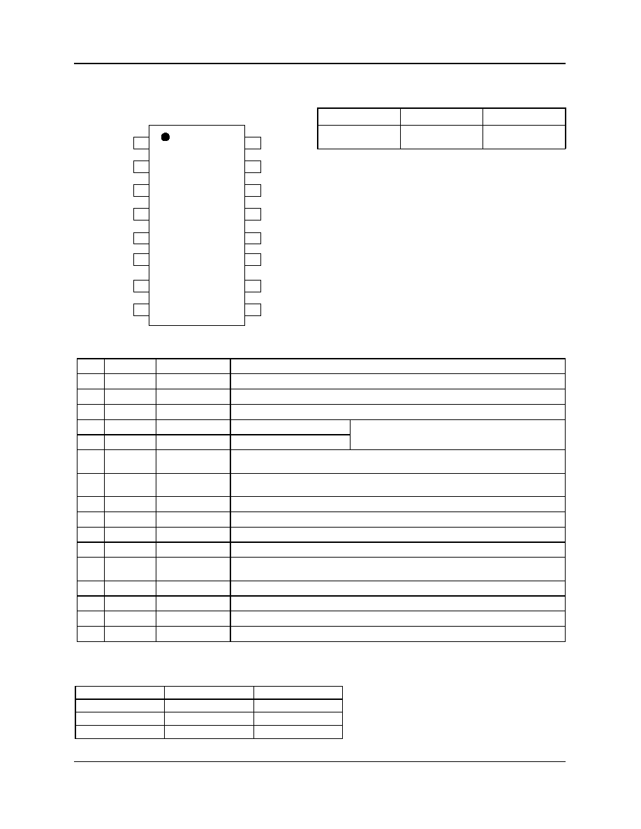
PIN CONFIGURATION
ORDERING INFORMATION
DEVICE
TEMP. RANGE
PACKAGE
XWM8181CDW
0 to 70
o
C
16-pin SOIC wide
body
DVDD
AGND2
2
15
AVDD
AGND1
1
16
DOUT
VREFIN
3
14
M C L K
VINP
4
13
VSMP
VINM
5
12
CLAMP
VRB
6
11
D G N D
VRT
7
10
9
8
N C
N C
PIN DESCRIPTION
PIN
NAME
TYPE
DESCRIPTION
1
AGND1
Ground
General analogue ground (0V).
2
AGND2
Ground
Reference analogue ground (0V).
3
VREFIN
Analogue input
Allows external control of the ADC references.
4
VINP
Analogue input
Positive video input
5
VINM
Analogue input
Negative video input
Usually one of VINP or VINM will be an externally
applied d.c. bias, the other will be a signal voltage.
6
VRB
Analogue output
Lower reference voltage. This pin must be connected to AGND and VRT via
decoupling capacitors. See Recommended External Components section for details.
7
VRT
Analogue output
Upper reference voltage. This pin must be connected to AGND and VRB via
decoupling capacitors. See Recommended External Components section for details.
8
NC
No internal connection
9
NC
No internal connection
10
DGND
Ground
Digital ground (0V).
11
CLAMP
Digital input
Connects VINP and VINM together, active high.
12
VSMP
Digital input
Video sample synchronisation pulse, at input pixel rate. Sampled on rising edge of
MCLK. See Operational Timing Diagrams for details.
13
MCLK
Digital input
Master clock. This clock can be applied at either 12 or 16 times the input pixel rate.
14
DOUT
Digital output
ADC serial data output, changes on falling edge of MCLK.
15
DVDD
Supply
Digital supply (3.3V, 5V).
16
AVDD
Supply
Analogue supply (3.3V, 5V).
POSSIBLE POWER SUPPLY COMBINATIONS
COMBINATION
AVDD (VOLTS)
DVDD (VOLTS)
1
5
5
2
3.3
3.3
3
5
3.3
Advanced Information
WM8181
WOLFSON MICROELECTRONICS LTD
AI Rev 3.0 January 2000
3
ABSOLUTE MAXIMUM RATINGS
Absolute Maximum Ratings are stress ratings only. Permanent damage to the device may be caused by continuously operating at
or beyond these limits. Device functional operating limits and guaranteed performance specifications are given under Electrical
Characteristics at the test conditions specified.
ESD Sensitive Device. This device is manufactured on a CMOS process. It is therefore generically susceptible
to damage from excessive static voltages. Proper ESD precautions must be taken during handling and storage
of this device.
CONDITION
MIN
MAX
Digital supply voltage: DVDD
GND - 0.3V
GND + 7V
Analogue supply voltage: AVDD
GND - 0.3V
GND + 7V
Digital ground: DGND. Analogue ground: AGND1, AGND2
GND - 0.3V
GND + 0.3V
Digital inputs: MCLK, VSMP, CLAMP
GND - 0.3V
DVDD + 0.3V
Digital outputs: DOUT
GND - 0.3V
DVDD + 0.3V
Analogue inputs: VINM, VINP, VREFIN
GND - 0.3V
AVDD + 0.3V
Reference pins: VRT, VRB
GND - 0.3V
AVDD + 0.3V
Operating temperature range: T
A
0
o
C
+70
o
C
Storage temperature
-65
o
C
+150
o
C
Package body temperature (soldering 10 seconds)
+240
o
C
Package body temperature (soldering 2 minutes)
+183
o
C
Notes: 1. GND denotes the voltage of any ground pin.
2. AGND and DGND pins are intended to be operated at the same potential. Differential voltages between these pins will
degrade performance.
RECOMMENDED OPERATING CONDITIONS
PARAMETER
SYMBOL
TEST CONDITIONS
MIN
TYP
MAX
UNIT
Operating temperature range
T
A
0
70
�
C
Analogue supply voltage (5V)
AVDD
4.5
5.0
5.5
V
Analogue supply voltage (3.3V)
AVDD
2.97
3.3
3.63
V
Digital input and output
supply voltage
DVDD
2.97
3.3
AVDD
V
WM8181
Advanced Information
WOLFSON MICROELECTRONICS LTD
AI Rev 3.0 January 2000
4
ELECTRICAL CHARACTERISTICS
TEST CHARACTERISTICS
AVDD = DVDD = 2.97 to 3.63V and 4.5 to 5.5V, AGND1 = AGND2 = DGND = 0V, T
A
= 0 to 70
�
C, MCLK = 24MHz
unless otherwise stated.
PARAMETER
SYMBOL
TEST
CONDITIONS
MIN
TYP
MAX
UNIT
ANALOGUE SPECIFICATION
12-bit ADC including Sample and Hold. No Missing Codes Guaranteed.
Maximum sample rate
MCLK:VSMP ratio = 12:1
2
MSPS
Input signal voltage for
ADC full-scale (internal
reference control)
VINP-VINM
1.5
V
Input signal voltage for
ADC full-scale (external
reference control)
VINP-VINM
VREFIN
V
Input signal voltage for
ADC zero-scale (internal
reference control)
VINP-VINM
0
V
Input signal voltage for
ADC zero-scale (external
reference control)
VINP-VINM
0
V
Differential non-linearity
DNL
0.5
LSB
Integral non-linearity
INL
1.5
LSB
Analogue Inputs
Input voltage limits
VINP, VINM
0
AVDD
V
References: VRT, VRB
AVDD = 5V
2.85
V
VRT (internal reference control)
AVDD = 3.3V
1.70
V
AVDD = 5V
1.35
V
VRB (internal reference control)
AVDD = 3.3V
0.95
V
AVDD = 5V
2.10 +
VREFIN/2
V
VRT (external reference control)
AVDD = 3.3V
1.35 +
VREFIN/4
V
AVDD = 5V
2.10 -
VREFIN/2
VRB (external reference control)
AVDD = 3.3V
1.35 -
VREFIN/4
V
VRT, VRB output leakage
Power down
<1
�A
Clamp
VINM to VINP leakage
CLAMP low
<1
�A
VINM to VINP resistance
CLAMP high, AVDD = 3.3V
VINP = VINM = 2V
50
VINM to VINP resistance
CLAMP high, AVDD = 5V
VINP = VINM = 1.4V
30

Advanced Information
WM8181
WOLFSON MICROELECTRONICS LTD
AI Rev 3.0 January 2000
5
TEST CHARACTERISTICS
AVDD = DVDD = 2.97 to 3.63V and 4.5 to 5.5V, AGND1 = AGND2 = DGND = 0V, T
A
= 0 to 70
�
C, MCLK = 24MHz
unless otherwise stated.
PARAMETER
SYMBOL
TEST
CONDITIONS
MIN
TYP
MAX
UNIT
DIGITAL SPECIFICATION
Digital Inputs
High level input voltage
V
IH
0.8
DVDD
V
Low level input voltage
V
IL
0.2
DVDD
V
High level input current
<1
�A
Low level input current
<1
�A
Input capacitance
5
pF
Digital Outputs
High level output voltage
I
OH
= 1mA
DVDD - 0.5
V
Low level output voltage
I
OL
= -1mA
0.5
V
High impedance output current
<1
�A
OVERALL SYSTEM SPECIFICATION
Supply Currents
Total analogue supply current �
active
AVDD = DVDD = 5V
AVDD = DVDD = 3.3V
21
19
mA
mA
Total digital supply current �
active
AVDD = DVDD = 5V
AVDD = DVDD = 3.3V
2
1
mA
mA
Supply current � disabled
AVDD = DVDD = 5V
AVDD = DVDD = 3.3V
<1
<1
�A
�A
M C L K
V S M P
DOUT
t
M C L K H
t
M C L K L
t
PER
t
V S M P S U
t
V S M P H
S A M P L E n
t
P D
n-2 D[11]
n-2 D[10]
n-2 D[9]
Figure 1 Clock Inputs and Data Output
TEST CHARACTERISTICS
AVDD = DVDD = 2.97 to 3.63V and 4.5 to 5.5V, AGND1 = AGND2 = DGND = 0V, T
A
= 0 to 70
�
C, MCLK = 24MHz
unless otherwise stated.
PARAMETER
SYMBOL
TEST CONDITIONS
MIN
TYP
MAX
UNIT
Maximum MCLK period
t
PER
41.7
ns
MCLK high
t
MCLKH
16
ns
MCLK low
t
MCLKL
16
ns
VSMP data set-up time
t
VSMPSU
10
ns
VSMP data hold time
t
VSMPH
10
ns
MCLK to DOUT
propagation delay
t
PD
AVDD = DVDD = 5V
10
ns
MCLK to DOUT
propagation delay
t
PD
AVDD = DVDD = 3.3V
15
ns
Note: Parameters are measured at 50% of the rising/falling edge.

WM8181
Advanced Information
WOLFSON MICROELECTRONICS LTD
AI Rev 3.0 January 2000
6
M C L K
V S M P
DOUT
D O N ' T C A R E
64 MCLK Rising Edges
t
P Z D
Hi-Z
t
PZE
t
P D
Hi-Z
Figure 2 Power Down/Power Up
TEST CHARACTERISTICS
AVDD = DVDD = 2.97 to 3.63V and 4.5 to 5.5V, AGND1 = AGND2 = DGND = 0V, T
A
= 0 to 70
�
C, MCLK = 24MHz
unless otherwise stated.
PARAMETER
SYMBOL
TEST CONDITIONS
MIN
TYP
MAX
UNIT
VSMP to DOUT enabled
t
PZE
10
ns
VSMP to DOUT enabled
t
PZE
AVDD = DVDD = 3.3V
10
ns
MCLK to DOUT disabled
t
PZD
10
ns
MCLK to DOUT disabled
t
PZD
AVDD = DVDD = 3.3V
10
ns
MCLK to DOUT
propagation delay
t
PD
10
ns
MCLK to DOUT
propagation delay
t
PD
AVDD = DVDD = 3.3V
15
ns
Note:
Parameters are measured at 50% of the rising/falling edge.
MCLK
VSMP
INPUT
VIDEO
(CCD)
t
V S U
t
V H
VIDEO
(CIS)
Figure 3 Input Video Timing
TEST CHARACTERISTICS
AVDD = DVDD = 2.97 to 3.63V and 4.5 to 5.5V, AGND1 = AGND2 = DGND = 0V, T
A
= 0 to 70
�
C, MCLK = 24MHz
unless otherwise stated.
PARAMETER
SYMBOL
TEST CONDITIONS
MIN
TYP
MAX
UNIT
Input video set-up time
t
VSU
10
ns
Input video hold time
t
VH
20
ns
Notes: 1.
t
VSU
and t
RSU
denote the set-up time required from when the input video signal has settled.
2.
Parameters are measured at 50% of the rising/falling edge.

Advanced Information
WM8181
WOLFSON MICROELECTRONICS LTD
AI Rev 3.0 January 2000
7
DEVICE DESCRIPTION
INTRODUCTION
The WM8181 is a serial output ADC that is designed to digitise analogue signals directly from CIS
and CCD sensors. The reset or reference level and video level from the sensor outputs are sampled
using an internal Sample and Hold circuit with an optional black level Clamp. The difference between
the sampled levels is passed onto a pipeline ADC with internally generated references where it is
converted into a 12-bit digital output. Please refer to the block diagram shown on page 1.
GENERAL OPERATION
SAMPLE AND HOLD
The WM8181 Sample and Hold samples signals from the VINP and VINM inputs. VINM and VINP
are connected to the sensor video output and a black level reference. No external buffering is
required as long as the input signals have settled before the samples are taken. The black level
reference can be provided by either the sensor or a separate circuit. Both inputs are sampled
simultaneously and the difference is passed on to the ADC to be converted.
For positive-going sensor outputs, VINP is used to input the video signal and VINM is used as the
black level reference. For negative-going sensor outputs, VINM is used as the video input and VINP
is used as the black level reference.
CLAMP
For a.c. (capacitively) coupled CCD signals, VINP and VINM may be connected together via the
optional internal clamp switch, which is controlled by the CLAMP pin. The switch is closed during the
reset period of the sensor output and open during the video period, allowing reset level clamping to
be performed. This ensures that the input signal is maintained within the input voltage limits of the
device, and that the true value of the video signal is processed.
ADC
The ADC converts the differential output from the Sample and Hold into 12-bit digital data ensuring
no missing codes in the final digitised output. The 12-bit parallel output from the ADC is transformed
into serial format, which is available to the user at the DOUT pin, MSB first.
REFERENCES
The WM8181 has internally generated references, which are controlled via the VREFIN pin. These
references are used to set the upper (VRT) and lower limits (VRB) of the ADC range and the full-
scale input range (VINP � VINM) of the device.
If VREFIN is tied to AVDD, the internal bandgap generator is used to determine the full-scale range.
If VREFIN is not tied to AVDD, the full-scale range is determined by the voltage on the VREFIN pin.
This is shown in Table 1. The ADC reference voltages, VRT and VRB, are driven onto the VRT and
VRB pins by internal amplifiers in the WM8181. Only external decoupling capacitors are required for
the VRT and VRB pins.
SUPPLY (V)
VREFIN (V)
REFERENCE
CONTROL
INPUT VOLTAGE
(VINP-VINM) FOR
ZERO (0) OUTPUT
CODE
INPUT VOLTAGE (VINP-
VINM) FOR FULL-SCALE
(+4095) OUTPUT CODE
5
AVDD
Internal
0
1.5
5
0.5 - 2
External
0
VREFIN
3.3
AVDD
Internal
0
1.5
3.3
0.75 � 1.5
External
0
VREFIN
Table 1
VREFIN and ADC Input Voltage Requirements for Internal and External
Reference Control

WM8181
Advanced Information
WOLFSON MICROELECTRONICS LTD
AI Rev 3.0 January 2000
8
OVERALL TIMING
The WM8181 input sampling, conversion and data output is controlled by externally applied MCLK
and VSMP clocks. Please refer to the Operational Timing Diagrams (Figures 4 and 5) shown at the
end of this section.
12:1 MCLK: VSMP RATIO OPERATION
MCLK can run at speeds of up to 24MHz. VSMP is a pulse one MCLK period long, with 12 times the
period of MCLK. VSMP must cover one rising edge of MCLK.
If VSMP is high for more than one MCLK rising edge, the last MCLK rising edge that is covered is
defined as the starting point and the video signal will be sampled on the next rising edge of MCLK.
Output data being processed at this time may be corrupted.
VSMP should be held low for 11 MCLK rising edges, then pulsed high for the 12th MCLK rising edge
to produce an MCLK:VSMP ratio of 12:1. If VSMP is held low for less than 11 MCLK rising edges,
the device will reset to the starting point and the video signal will be sampled on the next rising edge
of MCLK. Output data being processed during this time may be corrupted.
16:1 MCLK: VSMP RATIO OPERATION
The WM8181 can also operate with an MCLK:VSMP ratio of 16:1. Video signal sampling is
performed in the same manner as in 12:1 operation except that the device will wait an extra four
MCLK periods for the next VSMP pulse to go low before sampling the video signal.
DEVICE LATENCY
For 12:1 operation, the WM8181 will start to output valid data MSB first on the falling edge of MCLK
24.5 MCLK periods after the sampling instant (first rising edge of MCLK after VSMP goes low) for
that pixel. The device continues to output the data on the next 11 falling edges of MCLK
For 16:1 operation, the output latency increases to 32.5 MCLK periods after the sampling instant.
Data is output MSB first on this falling edge of MCLK, and continues over the next 11 falling edges of
MCLK. The four bits between the end of one output and the start of the next will be 0.
POWER DOWN
If VSMP is held high for 64 MCLK rising edges, the device will power down, causing DOUT, VRT,
and VRB to change into a high impedance state. The device will start powering up immediately on
VSMP going low, however VRT and VRB will take some time to recover and settle, depending on
how their voltages have decayed during power down and the decoupling capacitors used. Typically
for 1
�
F decoupling capacitors the amount of time taken for VRT and VRB to recover may be up to
10ms. If 0.1
�
F capacitors are used, this time will decrease to typically 1ms.
OPERATIONAL TIMING DIAGRAMS
C C D
Outputs
V S M P
S/H
R e s e t
D O U T
M C L K
R e s e t
Video Pixel 1
R e s e t
Video Pixel 2
Video Pixel 3
D 1 1
D0 PIXEL - 2
D 1 1
D0 PIXEL - 1
D 1 1
D0 PIXEL 0
L A T E N C Y = 2 4 . 5 M C L K P E R I O D S
Video Pixel 0
Figure 4 12:1 Operation

Advanced Information
WM8181
WOLFSON MICROELECTRONICS LTD
AI Rev 3.0 January 2000
9
C C D
Outputs
V S M P
S/H
R e s e t
D O U T
M C L K
R e s e t
Video Pixel 1
R e s e t
Video Pixel 2
Video Pixel 3
D 1 1
D0 PIXEL - 2
D 1 1
D0 PIXEL - 1
D 1 1
D0 PIXEL 0
L A T E N C Y = 3 2 . 5 M C L K P E R I O D S
0 0 0 0
0 0 0 0
0 0 0 0
Video Pixel 0
Figure 5 16:1 Operation
APPLICATIONS RECOMMENDATIONS
INTRODUCTION
The WM8181 is a mixed signal device, therefore careful PCB layout is required. The following
section contains PCB layout guidelines, which are recommended for optimal performance from the
WM8181, and some typical application circuits.
PCB LAYOUT
1)
Use separate analogue and digital power and ground planes. The analogue and digital ground
planes should be connected as close as possible to, or underneath, the WM8181.
2)
Place all supply decoupling capacitors as close as possible to their respective supply pins and
provide a low impedance path from the capacitors to the appropriate ground.
3)
Avoid noise on AGND pins 1 and 2.
4) Avoid noise on reference pins VRT and VRB. Place the decoupling capacitors as close as
possible to these pins and provide a low impedance path from the capacitors to analogue
ground.
5)
When VREFIN is used as an external reference control, any noise on VREFIN will degrade the
performance of the ADC. In this case, VREFIN must be carefully de-coupled to AGND.
6)
Minimise load capacitance on digital output DOUT. Capacitive loads of greater than 20pF will
degrade performance. Use buffers if necessary and keep tracks short.
TYPICAL APPLICATIONS
The WM8181 is intended for colour scanner applications using a line-by-line architecture and
monochrome scanners, as used in fax machines.
The low pincount and simple digital interface gives the scanner designer the opportunity to place the
ADC near to the sensor. This allows the video information to be converted into the digital domain as
early as possible in the signal chain and minimises analogue noise problems. In the typical
architecture of a flatbed scanner, this means that only power and digital signals appear on the ribbon
minimising crosstalk between the digital clocks and analogue video signals. Care must be taken to
avoid any increase in EMI generated by the higher clock rates on the ribbon cable.
CIS SCANNER
The WM8181 is ideal for use in CIS based scanners where the video output is supplied on a single
output pin. This is true of the majority of colour CIS and all monochrome CIS.
In general, CIS devices provide a video output that becomes more positive for more illumination. This
situation corresponds to the d.c. Coupled Positive Video diagram, Figure 6. The value of the black
reference voltage should be set to be slightly less than the black level output from the CIS to ensure
that the black never saturates.

WM8181
Advanced Information
WOLFSON MICROELECTRONICS LTD
AI Rev 3.0 January 2000
10
S Y S T E M
A S I C
C I S
S E N S O R
V
O U T
WM8181
V S M P
D O U T
M C L K
V I N P
V I N M
C L A M P
V R E F I N
V R T
V R B
E X A C T C I R C U I T R Y
M A Y V A R Y
D E P E N D I N G O N
S E N S O R U S E D
B L A C K
R E F E R E N C E
L E V E L
S E T V O L T A G E T O M A T C H V
P P
F R O M
S E N S O R O R T I E T O A V D D T O S E T
F U L L - S C A L E I N P U T T O 1 . 5 V
Figure 6 d.c. Coupled Positive Video
Some of the newer CIS devices have a reference voltage that corresponds closely to the black level.
In most cases this reference voltage cannot be applied directly to the VINM pin because the black
video output can go below this value and will be outside the range of the ADC. To overcome this,
VINM should be driven from a voltage that is slightly more negative than the CIS reference voltage.
This is shown in Figure 7. The input current to VINM is small but care should be taken to ensure that
R2 and R3 do not load the CIS reference circuit.
S Y S T E M
A S I C
C I S
S E N S O R
V
O U T
WM8181
V S M P
D O U T
M C L K
V I N P
V I N M
C L A M P
V
R E F
V R E F I N
V R T
V R B
E X A C T C I R C U I T R Y
M A Y V A R Y
D E P E N D I N G O N
S E N S O R U S E D
S E T V O L T A G E T O M A T C H V
P P
F R O M
S E N S O R O R T I E T O A V D D T O S E T
F U L L - S C A L E I N P U T T O 1 . 5 V
Figure 7 CIS with Reference Voltage

Advanced Information
WM8181
WOLFSON MICROELECTRONICS LTD
AI Rev 3.0 January 2000
11
CCD SCANNER
The differential nature of the WM8181 allows it to interface as easily to CCD sensors as to CIS. The
negative going video simply requires that the VINP and VINM pins are swapped over so that the
video signal is applied to VINM and the reference voltage is applied to VINP. The d.c. level of the
CCD output must lie within the input limits of the WM8181. A level shifter may be required to ensure
this. See Figure 8.
S Y S T E M
A S I C
C C D
S E N S O R
V
O U T
WM8181
V S M P
D O U T
M C L K
V I N P
V I N M
C L A M P
V R E F I N
V R T
V R B
B L A C K
R E F E R E N C E
L E V E L
L E V E L
S H I F T
L E V E L S H I F T
D E P E N D E N T O N
V
O U T
D C L E V E L
S E T V O L T A G E T O M A T C H
V
P P
F R O M S E N S O R .
Figure 8 d.c. Coupled Negative Video
USING THE INTERNAL CLAMP
When using a CCD it is recommended that the designer use a.c. (capacitive) coupling between the
CCD output buffer and the input to the WM8181, shown in Figure 9. A CCD sensor has a negative
going video signal superimposed on a d.c. voltage of around 6V. The series capacitor between the
CCD buffer and the input to the WM8181 removes this large d.c. voltage while still allowing the video
signal through.
S Y S T E M
A S I C
C C D
S E N S O R
V
O U T
WM8181
V S M P
D O U T
M C L K
V I N P
V I N M
C L A M P
V R E F I N
V R T
V R B
4 . 7 k
4 . 7 k
2 2 0 n
2 0 0 p
S E T V O L T A G E T O M A T C H
V
P P
F R O M S E N S O R .
Figure 9 a.c. Coupled Negative Video

WM8181
Advanced Information
WOLFSON MICROELECTRONICS LTD
AI Rev 3.0 January 2000
12
During the reset period of the video waveform the user applies a logic high signal to the CLAMP pin,
connecting the VINP pin to the VINM pin. This is illustrated in Figure 10. This has the effect of
charging, or discharging, the VINM side of the coupling capacitor to the black reference voltage
applied to VINP. When the CLAMP pin is taken low again the voltage across the capacitor will stay at
a fixed value and the input to the WM8181 will follow the output from the CCD. The WM8181
therefore converts the true value of the video signal, V
RS
� V
VS
.
V
R S
V
V S
C L O S E D
O P E N
C L O S E D
C L O S E D
O P E N
O P E N
V ID E O
S IG N A L
C L A M P
S W IT C H
C L A M P
Figure 10 Clamp Switch Operation.
ADJUSTING THE ADC INPUT RANGE
The WM8181 normally uses an internal bandgap reference to generate the ADC reference voltages.
With the recommended decoupling on the VRT and VRB pins, this ensures that the ADC receives
the cleanest reference voltages and thus achieves the optimum performance. The full scale input
range of the ADC is fixed in this mode to be 1.5V and is largely independent of supply voltage
variations. VREFIN should be connected to AVDD in this case.
It is possible to adjust the input range of the ADC by applying an externally generated voltage to the
VREFIN pin. The value of the ADC references and the corresponding input range of the ADC can be
determined from Table 1 in the Device Description section of this datasheet. Care must be taken to
avoid any noise on the VREFIN pin, as any noise on this pin with respect to AGND will degrade the
performance of the WM8181.
Advanced Information
WM8181
WOLFSON MICROELECTRONICS LTD
AI Rev 3.0 January 2000
13
RECOMMENDED EXTERNAL COMPONENTS
1 1
1 3
3
D V D D
D G N D
V I N P
V I N M
C L A M P
M C L K
V R E F I N
A G N D 2
A G N D 1
A V D D
C l a m p
Control
R e f e r e n c e
Control
1 4
D O U T
O u t p u t D a t a
7
6
V R B
V R T
C
3
D G N D
D V D D
C
7
A G N D
A V D D
C
8
C
4
C
6
C
5
A G N D
R e f e r e n c e s
1 6
1
2
A V D D
1 5
1 0
D V D D
C
1
4
5
V i d e o
Inputs
1 2
V S M P
T i m i n g
S i g n a l s
W M 8 1 8 1
C
1
to C
6
should be fitted as close to
N O T E S :
A G N D a n d D G N D s h o u l d b e c o n n e c t e d
as close to WM8181 as possible.
W M 8 1 8 1 a s p o s s i b l e .
1.
2.
C
2
+
+
Figure 6 Recommended External Components Diagram
COMPONENT
REFERENCE
SUGGESTED
VALUE
DESCRIPTION
C1
0.1
�
F
Decoupling for DVDD.
C2
0.1
�
F
Decoupling for AVDD.
C3
0.1
�
F
High frequency decoupling between VRT and VRB.
C4
1
�
F
Low frequency decoupling between VRT and VRB (non-polarised, optional).
C5
0.1
�
F
Decoupling for VRB.
C6
0.1
�
F
Decoupling for VRT.
C7
10
�
F
Reservoir capacitor for DVDD.
C8
10
�
F
Reservoir capacitor for AVDD.
Table 2 External Components Description
WM8181
Advanced Information
WOLFSON MICROELECTRONICS LTD
AI Rev 3.0 January 2000
14
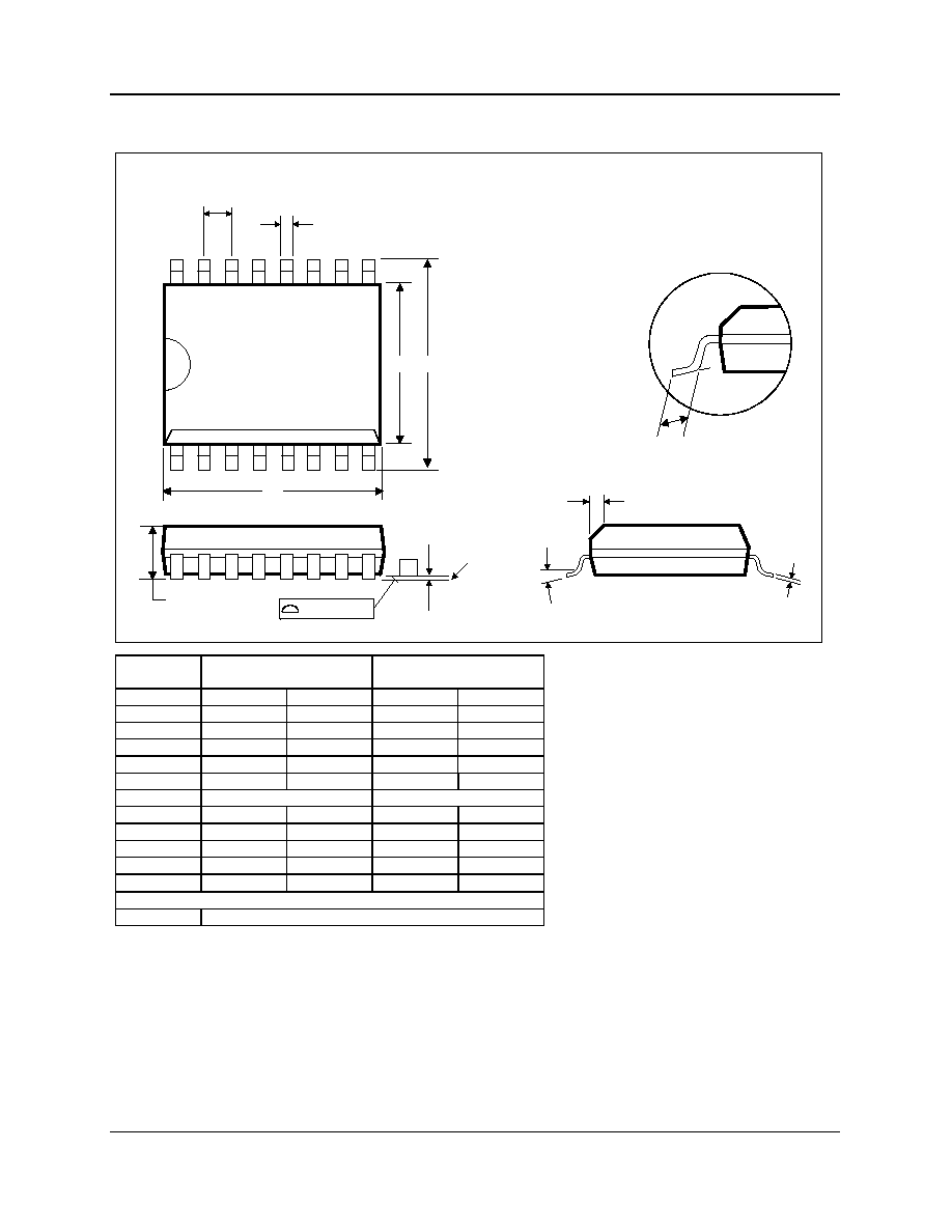
PACKAGE DIMENSIONS
Symbols
Dimensions
(mm)
Dimensions
(Inches)
MIN
MAX
MIN
MAX
A
2.35
2.65
0.0926
0.1043
A
1
0.10
0.30
0.0040
0.0118
B
0.33
0.51
0.0130
0.0200
C
0.23
0.32
0.0091
0.0125
D
10.10
10.50
0.3465
0.3622
e
1.27 BSC
0.0500 BSC
E
7.40
7.60
0.2914
0.2992
h
0.25
0.75
0.0100
0.0290
H
10.00
10.65
0.3940
0.4190
L
0.40
1.27
0.0160
0.0500
0
o
8
o
0
o
8
o
REF:
JEDEC.95, MS-013
NOTES:
A. ALL LINEAR DIMENSIONS ARE IN MILLIMETERS (INCHES).
B. THIS DRAWING IS SUBJECT TO CHANGE WITHOUT NOTICE.
C. BODY DIMENSIONS DO NOT INCLUDE MOLD FLASH OR PROTRUSION, NOT TO EXCEED 0.25MM (0.010IN).
D. MEETS JEDEC.95 MS-013, VARIATION = AA. REFER TO THIS SPECIFICATION FOR FURTHER DETAILS.
DM019.A
DW: 16 PIN SOICW 7.5mm (0.3") Wide Body, 1.27mm Lead Pitch
L
A
16
D
e
B
1
8
9
h x 45
o
C
E
H
SEATING PLANE
A1
-C-
0.10 (0.004)