 | –≠–ª–µ–∫—Ç—Ä–æ–Ω–Ω—ã–π –∫–æ–º–ø–æ–Ω–µ–Ω—Ç: XC3100A | –°–∫–∞—á–∞—Ç—å:  PDF PDF  ZIP ZIP |

2-177
XC3100A
Logic Cell
Array Families
Features
∑ Ultra-high-speed FPGA family with six members
≠ 50-85 MHz system clock rates
≠ 190 to 325 MHz guaranteed flip-flop toggle rates
≠ 1.75 to 4.1 ns logic delays
∑ High-end additional family member in the 22 X 22
CLB array-size XC3195A device
∑ 8 mA output sink current and 8 mA source current
∑ Maximum power-down and quiescent current is 5 mA
∑ Both families are 100% architecture and pin-out
compatible with other XC3000 families
∑ Beyond this, XC3100A is also software and bitstream
compatible with the XC3000, XC3000A, and XC3000L
families
∑ 100% PCI complaint (A-2 speed grade in plastic quad
flat pack (PQFP) packaging).
XC3100A combines the features of the XC3000A and
XC3100 families.
∑ Additional interconnect resources for TBUFs and CE
inputs
∑ Error checking of the configuration bitstream
∑ Soft startup holds all outputs slew-rate limited during
initial power-up
∑ More advanced CMOS process
Product Specifications
Æ
Description
The XC3100A is a performance-optimized relative of the
XC3000 and XC3000A families. While all families are
footprint compatible, XC3100A familiy extends the system
performance beyond 80 MHz.
The XC3100A familiy follows the XC4000 speed-grade
nomenclature, indicating device performance with a num-
ber that is based on the internal logic-block delay, in ns.
The XC3100A family offers the following enhancements
over the popular XC3100 family.
The XC3100A family has additional interconnect resources
to drive the I-inputs of TBUFs driving horizontal Longlines.
The CLB Clock Enable input can be driven from a second
vertical Longline. These two additions result in more
efficient and faster designs when horizontal Longlines are
used for data bussing.
During configuration, the XC3100A devices check the
bitstream format for stop bits in the appropriate positions.
Any error terminates the configuration and pulls INIT Low.
When the configuration process is finished and the device
starts up in user mode, the first activation of the outputs is
automatically slew-rate limited. This feature, called Soft
Startup, avoids the potential ground bounce when all
outputs are turned on simultaneously. After start-up, the
slew rate of the individual outputs is, as in all XC3000
families, determined by the individual configuration option.
The XC3100A family is a superset of the XC3000 families.
Any bitstream used to configure an XC3000, XC3000A,
XC3000L or XC3100 device, will configure the same-size
XC3100A device exactly the same way.
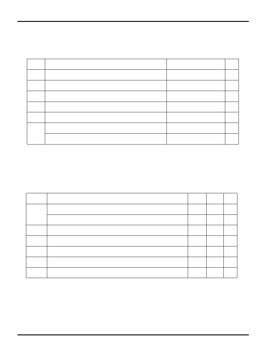
User I/O
Horizontal
Configuration
Device
CLBs
Array
Max
Flip-Flops
Longlines
Data Bits
XC3120A
64
8 x 8
64
256
16
14,779
XC3130A
100
10 x 10
80
360
20
22,176
XC3142A
144
12 x 12
96
480
24
30,784
XC3164A
224
16 x 14
120
688
28
46,064
XC3190A
320
16 x 20
144
928
40
64,160
XC3195A
484
22 x 22
176
1,320
44
94,944
XC3100, XC3100A Logic Cell Array Family
2-178
Symbol Description
Units
V
CC
Supply voltage relative to GND
≠0.5 to +7.0
V
V
IN
Input voltage with respect to GND
≠0.5 to V
CC
+0.5
V
V
TS
Voltage applied to 3-state output
≠0.5 to V
CC
+0.5
V
T
STG
Storage temperature (ambient)
≠65 to +150
∞
C
T
SOL
Maximum soldering temperature (10 s @ 1/16 in.)
+260
∞
C
Junction temperature plastic
+125
∞
C
T
J
Junction temperature ceramic
+150
∞
C
Note:
Stresses beyond those listed under Absolute Maximum Ratings may cause permanent damage to the device. These
are stress ratings only, and functional operation of the device at these or any other conditions beyond those listed
under Recommended Operating Conditions is not implied. Exposure to Absolute Maximum Ratings conditions for
extended periods of time may affect device reliability.
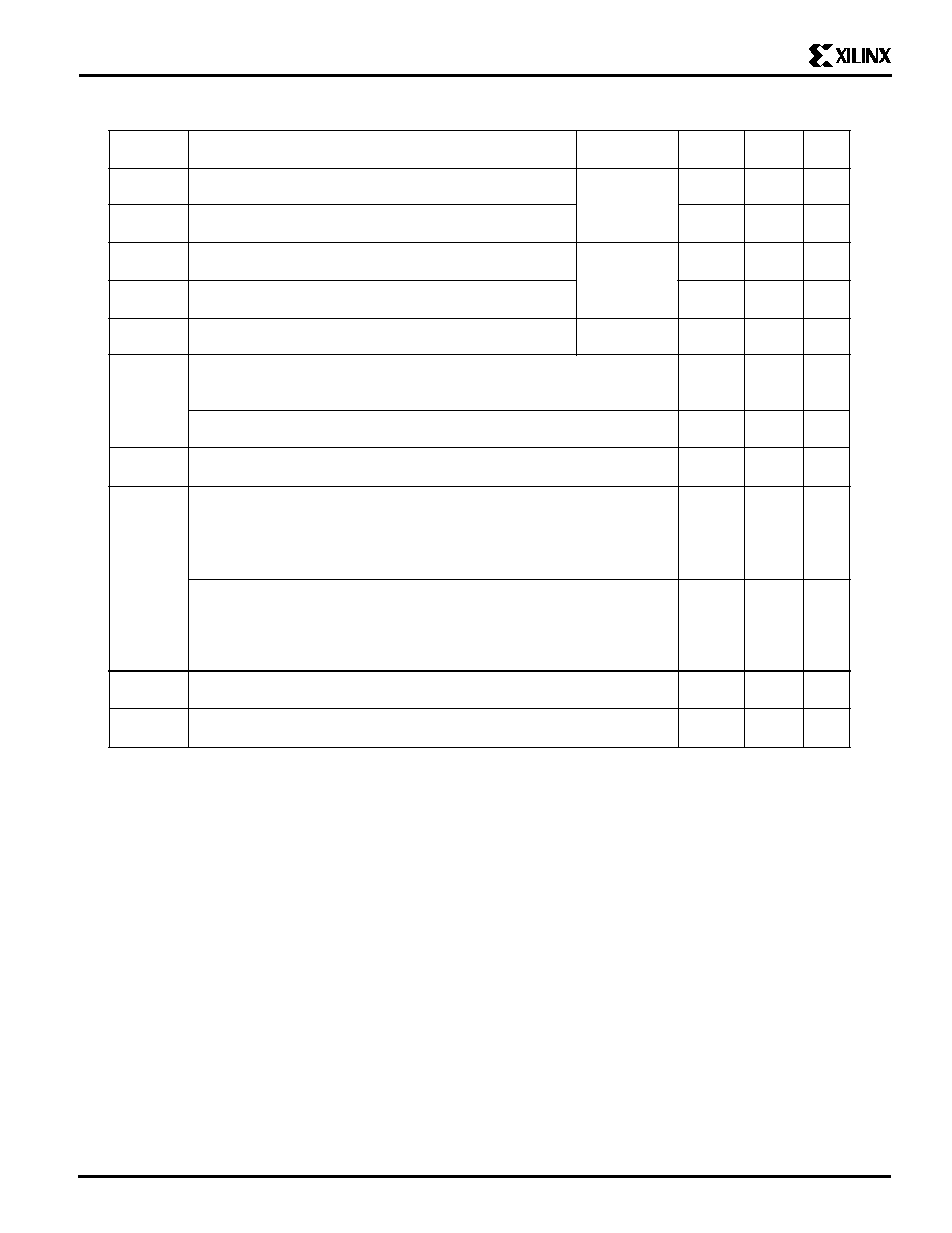
Symbol
Description
Min
Max
Units
V
CC
Supply voltage relative to GND Commercial 0
∞
C to +85
∞
C junction
4.75
5.25
V
Supply voltage relative to GND Industrial -40
∞
C to +100
∞
C junction
4.5
5.5
V
V
IHT
High-level input voltage -- TTL configuration
2.0
V
CC
V
V
ILT
Low-level input voltage -- TTL configuration
0
0.8
V
V
IHC
High-level input voltage -- CMOS configuration
70%
100%
V
CC
V
ILC
Low-level input voltage -- CMOS configuration
0
20%
V
CC
T
IN
Input signal transition time
250
ns
Absolute Maximum Ratings
Operating Conditions
Xilinx maintains test specifications for each product as controlled documents. To insure the use of the most recently
released device performance parameters, please request a copy of the current test-specification revision.
At junction temperatures above those listed as Operating Conditions, all delay parameters increase by 0.3% per
∞
C.
2-179
Symbol
Description
Min
Max
Units
V
OH
High-level output voltage (@ I
OH
= ≠8.0 mA, V
CC
min)
3.86
V
V
OL
Low-level output voltage (@ I
OL
= 8.0 mA, V
CC
min)
0.40
V
V
OH
High-level output voltage (@ I
OH
= ≠8.0 mA, V
CC
min
)
3.76
V
V
OL
Low-level output voltage (@ I
OL
= 8.0 mA, V
CC
min
)
0.40
V
V
CCPD
Power-down supply voltage (PWRDWN must be Low)
2.30
V
I
CCO
Quiescent LCA supply current
Chip thresholds programmed as CMOS levels
1
8
mA
Chip thresholds programmed as TTL levels
14
mA
I
IL
Input Leakage Current
≠10
+10
µ
A
C
IN
Input capacitance, all packages except PGA175
(sample tested)
All Pins except XTL1 and XTL2
10
pF
XTL1 and XTL2
15
pF
Input capacitance, PGA 175
(sample tested)
All Pins except XTL1 and XTL2
15
pF
XTL1 and XTL2
20
pF
I
RIN
Pad pull-up (when selected) @ V
IN
= 0V (sample tested)
0.02
0.17
mA
I
RLL
Horizontal long line pull-up (when selected) @ logic Low
0.20
2.80
mA
Note:
1. With no output current loads, no active input or long line pull-up resistors, all package pins at V
CC
or GND,
and the LCA configured with a MakeBits tie option.
2. Total continuous output sink current may not exceed 100 mA per ground pin. The number of ground pins varies
from two for the XC3120A in the PC84 package, to eight for the XC3195A in the PQ208 or PG223 package.
DC Characteristics Over Operating Conditions
Industrial
Commercial

XC3100, XC3100A Logic Cell Array Family
2-180
ADVANCE INFORMATION
Speed Grade
-5
-4
-3
-2
-1
Description
Symbol
Max
Max
Max
Max
Max
Global and Alternate Clock Distribution*
Either: Normal IOB input pad through clock buffer
to any CLB or IOB clock input
T
PID
6.8
6.5
5.6
5.2
4.8
Or:
Fast (CMOS only) input pad through clock
buffer to any CLB or IOB clock input
T
PIDC
5.4
5.1
4.3
4.0
3.8
TBUF driving a Horizontal Long line (L.L.)*
I to L.L. while T is Low (buffer active) (XC3100)
T
IO
4.1
3.7
3.1
(XC3100A)
T
IO
3.6
3.6
3.1
3.1
2.9
T
to L.L. active and valid with single pull-up resistor
T
ON
5.6
5.0
4.2
4.2
4.0
T
to L.L. active and valid with pair of pull-up resistors
T
ON
7.1
6.5
5.7
5.7
5.5
T
to L.L. High with single pull-up resistor
T
PUS
15.6
13.5
11.4
11.4
10.4
T
to L.L. High with pair of pull-up resistors
T
PUF
12.0
10.5
8.8
8.1
7.1
BIDI
Bidirectional buffer delay
T
BIDI
1.4
1.2
1.0
0.9
0.85
Buffer (Internal) Switching Characteristic Guidelines
* Timing is based on the XC3142A, for other devices see XACT timing calculator.
CLB Switching Characteristic Guidelines
1
T
ILO
CLB Output (X, Y)
(Combinatorial)
CLB Input (A,B,C,D,E)
CLB Clock
CLB Input
(Direct In)
CLB Input
(Enable Clock)
CLB Output
(Flip-Flop)
CLB Input
(Reset Direct)
CLB Output
(Flip-Flop)
8
T
CKO
X5424
13 T
T
RPW
9
T
RIO
4
T
DICK
6
T
ECCK
12 T
CL
2
T
ICK
3
T
CKI
11 T
CH
5
T
CKDI
7
T
CKEC
Units
ns
ns
ns
ns
ns
ns
ns
ns
ns

2-181
ADVANCE INFORMATION
Speed Grade
-5
-4
-3
-2
Description
Symbol
Min
Max
Min
Max
Min
Max
Min
Max
Combinatorial Delay
Logic Variables A, B, C, D, E,
to outputs X or Y
1
T
ILO
4.1
3.3
2.7
2.2
Sequential delay
Clock K to outputs X or Y
8
T
CKO
3.1
2.5
2.1
1.7
Clock K to outputs X or Y when Q is returned
through function generators F or G
to drive X or Y
T
QLO
6.3
5.2
4.3
3.5
Set-up time before clock K
Logic Variables
A, B, C, D, E
2
T
ICK
3.1
2.5
2.1
1.8
Data In
DI
4
T
DICK
2.0
1.6
1.4
1.3
Enable Clock
EC
6
T
ECCK
3.8
3.2
2.7
2.5
Reset Direct inactive
RD
1.0
1.0
1.0
1.0
Hold Time after clock k
Logic Variables
A, B, C, D, E
3
T
CKI
0
0
0
0
Data In
DI
5
T
CKDI
1.0
1.0
0.9
0.9
Enable Clock
EC
7
T
CKEC
1.0
0.8
0.7
0.7
Clock
Clock High time
11 T
CH
2.4
2.0
1.6
1.3
Clock Low time
12 T
CL
2.4
2.0
1.6
1.3
Max. flip-flop toggle rate
F
CLK
190
230
270
325
Reset Direct (RD)
RD width
13 T
RPW
3.8
3.2
2.7
2.3
delay from RD to outputs X or Y
9
T
RIO
4.4
3.7
3.1
2.7
Global Reset, from RESET Pad,
RESET width (Low)
(XC3142A)
T
MRW
14.0
14.0
12.0
12.0
delay from RESET pad to outputs X or Y
T
MRQ
17.0
14.0
12.0
12.0
CLB Switching Characteristic Guidelines (continued)
Testing of the switching parameters is modeled after testing methods specified by MIL-M-38510/605. All devices are 100%
functionally tested. Since many internal timing parameters cannot be measured directly, they are derived from benchmark timing
patterns. The following guidelines reflect worst-case values over the recommended operating conditions. For more detailed, more
precise, and more up-to-date timing information, use the values provided by the XACT timing calculator and used in the simulator.
Notes:
The CLB K to Q output delay (T
CKO
, #8) of any CLB, plus the shortest possible interconnect delay, is always longer than
the Data In hold time requirement (T
CKDI
, #5) of any CLB on the same die.
T
ILO
, T
QLO
and T
ICK
are specified for 4-input functions. For 5-input functions or base FGM functions, each of these
specifications for the XC3100A family increses by 0.50 ns (-5), 0.42 ns (-4) and 0.35 ns (-3).
Units
ns
ns
ns
ns
MHz
ns
ns
ns
ns
ns
ns
ns
ns
ns
ns
ns
ns
Min Max
1.75
1.4
3.2
1.7
1.2
2.3
1.0
0
0.8
0.6
1.3
1.3
325
2.3
2.4
12.0
12.0
-1

XC3100, XC3100A Logic Cell Array Family
2-182
IOB Switching Characteristic Guidelines
FLIP
FLOP
Q
D
R
SLEW
RATE
PASSIVE
PULL UP
OUTPUT
SELECT
3-STATE
INVERT
OUT
INVERT
FLIP
FLOP
or
LATCH
D
Q
R
REGISTERED IN
DIRECT IN
OUT
3- STATE
(OUTPUT ENABLE)
TTL or
CMOS
INPUT
THRESHOLD
OUTPUT
BUFFER
(GLOBAL RESET)
CK1
X3029
I/O PAD
Vcc
PROGRAM-CONTROLLED MEMORY CELLS
PROGRAMMABLE INTERCONNECTION POINT or PIP
=
IK
OK
Q
I
O
T
PROGRAM
CONTROLLED
MULTIPLEXER
CK2
3
T
PID
I/O Block (I)
I/O Pad Input
I/O Clock (IK/OK)
I/O Block (RI)
RESET
I/O Block (O)
I/O Pad TS
I/O Pad Output
I/O Pad Output
(Direct)
I/O Pad Output
(Registered)
X5425
5
T
OOK
12 T
IOL
1
T
PICK
11 T
IOH
4
T
IKRI
15 T
RPO
13 T
RRI
6
T
OKO
9
T
TSHZ
10 T
OP
7
T
OKPO
8
T
TSON

2-183
ADVANCE INFORMATION
IOB Switching Characteristic Guidelines (continued)
Testing of the switching parameters is modeled after testing methods specified by MIL-M-38510/605. All devices are 100%
functionally tested. Since many internal timing parameters cannot be measured directly, they are derived from benchmark timing
patterns. The following guidelines reflect worst-case values over the recommended operating conditions. For more detailed, more
precise, and more up-to-date timing information, use the values provided by the XACT timing calculator and used in the simulator.
Notes: 1. Timing is measured at pin threshold, with 50 pF external capacitive loads (incl. test fixture). For larger capacitive loads,
see XAPP 024. Typical slew rate limited output rise/fall times are approximately four times longer.
2. Voltage levels of unused (bonded and unbonded) pads must be valid logic levels. Each can be configured with the
internal pull-up resistor or alternatively configured as a driven output or driven from an external source.
3. Input pad set-up time is specified with respect to the internal clock (IK). In order to calculate system set-up time, subtract
clock delay (pad to ik) from the input pad set-up time value. Input pad holdtime with respect to the internal clock (IK) is
negative. This means that pad level changes immediately before the internal clock edge (IK) will not be recognized.
4. T
PID
, T
PTG
, and T
PICK
are 3 ns higher for XTAL2 when the pin is configured as a user input.
Speed Grade
-5
-4
-3
-2
Description
Symbol
Min
Max
Min Max
Min Max
Min Max
Propagation Delays (Input)
Pad to Direct In (I)
3
T
PID
2.8
2.5
2.2
2.0
Pad to Registered In (q) with
latch transparent
(XC3100A)
T
PTG
14.0
12.0
11.0
11.0
(XC3100)
T
PTG
16.0
15.0
13.0
Clock (IK) to Registered In (Q)
4
T
IKRI
2.8
2.5
2.2
1.9
Set-up Time (Input)
Pad to Clock (IK) set-up time
XC3100 Family
1
T
PICK
15.0
14.0
12.0
XC3120A,XC3130A
10.9
10.6
9.4
8.9
XC3142A
11.0
10.7
9.5
9.0
XC3164A
11.2
11.0
9.7
9.2
XC3190A
11.5
11.2
9.9
9.4
XC3195A
12.0
11.6
10.3
9.8
Propagation Delays (Output)
Clock (OK) to Pad
(fast)
7
T
OKPO
5.5
5.0
4.4
4.0
same
(slew-rate limited)
7
T
OKPO
14.0
12.0
10.0
9.7
Output (O) to Pad
(fast)
10 T
OPF
4.1
3.7
3.3
3.0
same (slew-rate limited) (XC3100A) 10 T
OPS
12.1
11.0
9.0
8.7
(XC3100)
10 T
OPF
13.0
11.0
9.0
3-state to Pad begin hi-Z (fast)
9
T
TSHZ
6.9
6.2
5.5
5.0
same
(slew-rate limited)
9
T
TSHZ
6.9
6.2
5.5
5.0
3-state to Pad active and valid (fast) (XC3100A)
8
T
TSON
10.0
10.0
9.0
8.5
same
(slew-rate limited)
8
T
TSON
18.0
17.0
15.0
14.2
3-state to Pad active and valid (fast) (XC3100)
8
T
TSON
12.0
10.0
9.0
same
(slew-rate limited)
8
T
TSON
20.0
17.0
15.0
Set-up and Hold Times (Output)
Output (O) to clock (OK) set-up time,(XC3100A)
5
T
OOK
5.0
4.5
4.0
3.6
(XC3100)
5
T
OOK
6.2
5.6
5.0
Output (O) to clock (OK) hold time
6
T
OKO
0
0
0
0
Clock
Clock High time
11 T
IOH
2.4
2.0
1.6
1.3
Clock Low time
12 T
IOL
2.4
2.0
1.6
1.3
Max. flip-flop toggle rate
F
CLK
190.0
230.0
270.0
325.0
Global Reset Delays
RESET Pad to Registered In (Q),
(XC3120/XC3120A)
13 T
RRI
18.0
15.0
13.0
13.0
(XC3195/XC3195A)
29.5
25.0
21.0
21.0
RESET Pad to output pad
(fast)
15 T
RPO
24.0
20.0
17.0
17.0
(slew-rate limited)
15 T
RPO
32.0
27.0
23.0
23.0
ns
ns
Units
ns
ns
ns
ns
ns
ns
ns
ns
ns
ns
ns
ns
ns
ns
ns
ns
ns
ns
ns
ns
ns
ns
ns
ns
MHz
ns
ns
ns
ns
Min-Max
1.8
11.0
1.8
8.5
8.6
8.8
9.0
9.4
3.6
8.9
2.7
8.0
4.5
4.5
6.5
11.8
3.2
0
1.3
1.3
325.0
13.0
21.0
17.0
22.0
-1
XC3100, XC3100A Logic Cell Array Family
2-184
For a detailed description of the device architecture, see pages 2-105 through 2-123.
For a detailed description of the configuration modes and their timing, see pages 2-124 through 2-132.
For detailed lists of package pin-outs, see pages 2-140 through 2-150.
For package physical dimensions and thermal data, see Section 4.
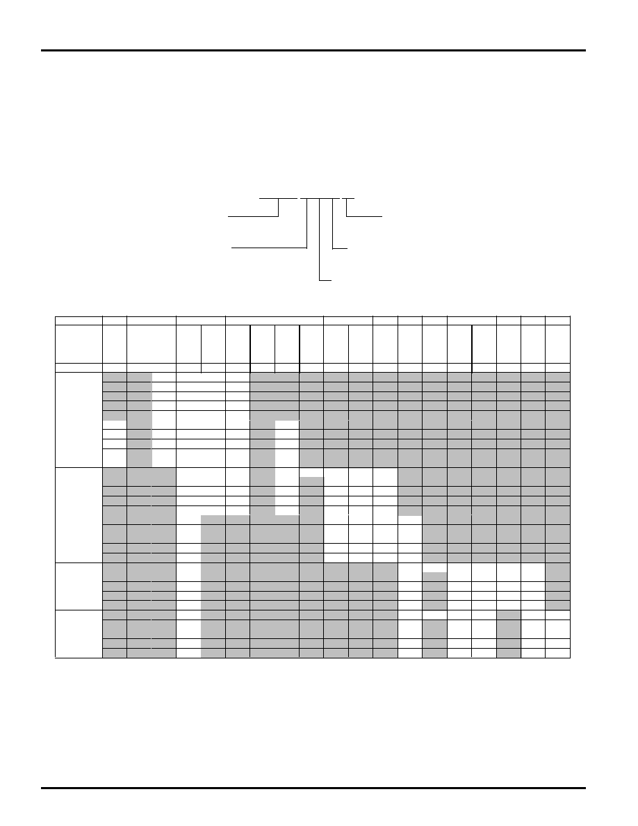
Ordering Information
Package Type
Example:
XC3130A-70PC44C
Toggle Rate
Device Type
Number of Pins
Temperature Range
PINS
44
64
68
84
100
132
144
160
164
175
176
208
223
TOP-
TOP-
TYPE
PLAST.
PLAST.
PLAST.
PLAST.
CERAM
PLAST.
PLAST.
PLAST. BRAZED PLAST. CERAM. PLAST.
PLAST. BRAZED PLAST. CERAM. PLAST.
PLAST. CERAM.
PLCC
VQFP
PLCC
PLCC
PGA
PQFP
TQFP
VQFP
CQFP
PGA
PGA
TQFP
PQFP
CQFP
PGA
PGA
TQFP
PQFP
PGA
CODE
PC44
VQ64
PC68
PC84
PG84
PQ100 TQ100 VQ100 CB100 PP132 PG132 TQ144 PQ160 CB164 PP175 PG175 TQ176 PQ208 PG223
-5
C I
C I
C I
C I
-4
C I
C I
C I
C I
XC3120A
-3
C I
C I
C I
C I
-2
C
C
C
C
-1
C
C
C
C
-5
C I
C I
C I
C I
C I
C
-4
C I
C I
C I
C I
C I
C
XC3130A
-3
C I
C I
C I
C I
C I
C
-2
C
C
C
C
C
C
-1
C
C
C
C
C
C
-5
C I
C I M B
C I
C
M B
C
C I M B
C I
-4
C I
C I
C I
C
C
C I
C I
XC3142A
-3
C I
C I
C I
C
C
C I
C I
-2
C
C
C
C
C
C
C
-1
C
C
C
C
C
C
C
-5
C I
C I
C I
C I
C I
-4
C I
C I
C I
C I
C I
XC3164A
-3
C I
C I
C I
C I
C I
-2
C
C
C
C
C
-1
C
C
C
C
C
-5
C I
C I
M B
C I
C I M B
C I
C I
-4
C I
C I
C I
C I
C I
C I
XC3190A
-3
C I
C I
C I
C I
C I
C I
-2
C
C
C
C
C
C
-1
C
C
C
C
C
C
-5
C I
C I
M B
C I
C I M B
C I
C I M B
-4
C I
C I
C I
C I
C I
C I
XC3195A
-3
C I
C I
C I
C I
C I
C I
-2
C
C
C
C
C
C
-1
C
C
C
C
C
C
C = Commercial = 0
∞
to +85
∞
C I = Industrial = -40
∞
to +100
∞
C M = Mil Temp = -55
∞
to +125
∞
C B = MIL-STD-883C Class B
Parentheses indicate future product plans
Component Availability