1
Zarlink Semiconductor Inc.
Features
�
16,384-channel x 16,384-channel non-blocking
unidirectional switching.The Backplane and
Local inputs and outputs can be combined to
form a non-blocking switching matrix with 64
stream inputs and 64 stream outputs.
�
8,192-channel x 8,192-channel non-blocking
Backplane to Local stream switch.
�
8,192-channel x 8,192-channel non-blocking
Local to Backplane stream switch.
�
8,192-channel x 8,192-channel non-blocking
Backplane input to Backplane output switch.
�
8,192-channel x 8,192-channel non-blocking
Local input to Local output stream switch.
�
Rate conversion on all data paths, Backplane to
Local, Local to Backplane, Backplane to
Backplane and Local to Local streams.
�
Backplane port accepts 32 ST-BUS streams
with data rates of 2.048Mb/s, 4.096Mb/s,
8.192Mb/s or 16.384Mb/s in any combination,
or a fixed allocation of 16 streams at
32.768Mb/s.
�
Local port accepts 32 ST-BUS streams with
data rates of 2.048Mb/s, 4.096Mb/s, 8.192Mb/s
or 16.384Mb/s, in any combination.
�
Per-stream channel and bit delay for Local input
streams.
�
Per-stream channel and bit delay for Backplane
input streams.
�
Per-stream advancement for Local output
streams.
�
Per-stream advancement for Backplane output
streams.
�
Constant throughput delay for frame integrity.
�
Per-channel high impedance output control for
Local and Backplane streams.
�
Per-channel driven-high output control for local
and backplane streams.
�
High impedance-control outputs for external
drivers on backplane and local port.
December 2002
Ordering Information
MT90869AG
272 Ball - PBGA
-40 to +85
o
C
MT90869
Flexible 16K Digital Switch (F16kDX)
Data Sheet
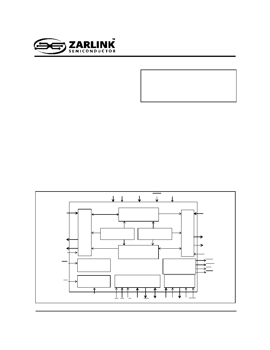
Figure 1 - MT90869 Functional Block Diagram
Backplane Data Memories
(8,192 channels)
DS CS R/W A14-A0 DTA D15-D0
Test Port
Microprocessor Interface
and Internal Registers
V
SS (GND)
V
DD_CORE
TDi TDo TCK TRST
TMS
LSTo0-31
(8,192 locations)
RESET
Local
Interface
Connection Memory
BSTi0-31
Backplane
Timing Unit
FP8i
PLL
LSTi0-31
Interface
Backplane
BSTo0-31
Local
C8i
V
DD_IO
LCST0-3
ODE
BCST0-3
C8o
C16o
FP8o
FP16o
V
DD_PLL
Local
Timing
Unit
(8,192 locations)
Connection Memory
Backplane
Interface
Local
Local Data Memories
(8,192 channels)
BORS
LORS

MT90869
Data Sheet
2
Zarlink Semiconductor Inc.
�
Per-channel message mode for local and backplane output streams.
�
Connection memory block programming for fast device initialization.
�
BER testing for local and backplane ports.
�
Automatic selection between ST-BUS and GCI-BUS operation.
�
Non-multiplexed Motorola microprocessor interface.
�
Conforms to the mandatory requirements of the IEEE-1149.1 (JTAG) standard.
�
Memory Built-In-Self-Test (BIST), controlled via microprocessor registers.
�
1.8V core supply voltage.
�
3.3V I/O supply voltage.
�
5V tolerant inputs, outputs and I/Os.
�
Per stream subrate switching at 4 bit, 2 bit and 1 bit depending on stream data rate.
Applications
�
Central Office Switches (Class 5)
�
Mediation Switches
�
Class-independent switches
�
Access Concentrators
�
Scalable TDM-Based Architectures
�
Digital Loop Carriers
Device Overview
The MT90869 has two data ports, the Backplane and the Local port. The Backplane port has two modes of
operation, either 32 input and 32 output streams operated at 2.048Mb/s, 4.096Mb/s, 8.192Mb/s or 16.384Mb/s, in
any combination, or 16 input and 16 output streams operated at 32.768Mb/s. The Local port has 32 input and 32
output streams operated at 2.048Mb/s, 4.096Mb/s, 8.192Mb/s or 16.384Mb/s, in any combination.
The MT90869 contains two data memory blocks (Backplane and Local) to provide the following switching path
configurations:
�
Backplane-to-Local, supporting 8K x 8K data switching,
�
Local-to-Backplane, supporting 8K x 8K data switching,
�
Backplane-to-Backplane, supporting 8K x 8K data switching.
�
Local-to-Local, supporting 8K x 8K data switching.
The device contains two connection memory blocks, one for the Backplane output and one for the Local output. Data
to be output on the serial streams may come from either of the data memories (Connection Mode) or directly from
the connection memory contents (Message Mode).
In Connection Mode the contents of the connection memory defines, for each output stream and channel, the source
stream and channel (stored in data memory) to be switched.
In Message Mode, microprocessor data can be written to the connection memory for broadcast on the output
streams on a per channel basis. This feature is useful for transferring control and status information to external
circuits or other ST-BUS devices.
The device uses a master frame pulse (FP8i) and master clock (C8i) to define the frame boundary and timing for
both the backplane port and the local port. The device will automatically detect whether an ST-BUS or a GCI-BUS
style frame pulse is being used. There is a two frame delay from the time RESET is de-asserted to the establishment
of full switch functionality. During this period the frame format is determined before switching begins.
The device provides FP8o, FP16o, C8o and C16o outputs to support external devices connected to the local port.

Data Sheet
MT90869
3
Zarlink Semiconductor Inc.
Subrate switching is accomplished by oversampling (i.e., 1 bit switching can be accomplished by sampling a 2 Mb/s
stream at 16 Mbps). Refer to MSAN 175.
A non-multiplexed Motorola microprocessor port allows programming of the various device operation modes and
switching configurations. The microprocessor port provides access for Register read/write, Connection Memory
read/write and Data Memory read-only operations. The port has a 15-bit address bus, 16-bit data bus and 4 control
signals. The microprocessor may monitor channel data in the backplane and local data memories.
The mandatory requirements of the IEEE-1149.1 (JTAG) standard are fully supported via a dedicated test port.
The MT90869 is manufactured in a 27mm x 27mm body, 1.27mm ball-pitch, 272-PBGA to JEDEC standard MS-
034 BAL-2 Iss. A.

Data Sheet
MT90869
5
Zarlink Semiconductor Inc.
Pin Description
Name
Package
Coordinates
Description
V
DD_IO
D6, D11, D15, F4,
F17, K4, L17, R4,
R17, U6, U10, U15
Power Supply for Periphery Circuits: +3.3V
V
DD_CORE
A7, B4, B12, D14,
K1, K20, N3, P18,
T17, U16, V1, V5,
Y7, Y11, Y14
Power Supply for Core Logic Circuits: +1.8V
V
DD_PLL
U12
Power Supply for Analogue PLL: +1.8V
V
SS (GND)
A1, D4, D8, D13,
D17, H4, H17, J9,
J10, J11, J12, K9,
K10, K11, K12, L9,
L10, L11, L12, M9,
M10, M11, M12, N4,
N17, U4, U8, U11,
U13, U17
Ground
BSTi0 - 15
K3, L1, L2, L3, L4,
M1, M2, M3, M4, N1,
N2, P1, P2, P3, P4,
R1
Backplane Serial Input Streams 0 to 15 (5V Tolerant, Internal pull-down). In
Non-32Mb/s Mode, these pins accept serial TDM data streams at a data-rate of:-
16.384 Mb/s (with 256 channels per stream),
8.192 Mb/s (with 128 channels per stream),
4.096 Mb/s (with 64 channels per stream), or
2.048Mb/s (with 32 channels per stream).
The data-rate is independently programmable for each input stream.
In 32Mb/s Mode, these pins accept serial TDM data streams at a fixed data-rate of
32.768 Mb/s (with 512 channels per stream).
BSTi16 - 31
R2, R3, T1, T2, T3,
T4, U1,W1, W2, W3,
Y1, Y2, U5, V4, W4,
Y4
Backplane Serial Input Streams 16 to 31 (5V Tolerant, Internal pull-down).
In Non-32Mb/s Mode, these pins accept serial TDM data streams at a data-rate
of:-
16.384 Mb/s (with 256 channels per stream),
8.192 Mb/s (with 128 channels per stream),
4.096 Mb/s (with 64 channels per stream), or
2.048Mb/s (with 32 channels per stream).
The data-rate is independently programmable for each input stream.
In 32Mb/s Mode, these pins are unused and should be externally connected to a
defined logic level.
BSTo0 - 15
C5, B5, A5 C4, A4,
A3, B1, B2, B3, C1,
C2, D1, D2, D3, E1,
E2
Backplane Serial Output Streams 0 to 15 (5V Tolerant, Three-state Outputs).
In Non-32Mb/s Mode, these pins output serial TDM data streams at a data-rate of:-
16.384 Mb/s (with 256 channels per stream),
8.192 Mb/s (with 128 channels per stream),
4.096 Mb/s (with 64 channels per stream), or
2.048Mb/s (with 32 channels per stream).
The data-rate is independently programmable for each output stream.
In 32Mb/s Mode, these pins output serial TDM data streams at a fixed data-rate of
32.768 Mb/s (with 512 channels per stream).
Refer to descriptions of the BORS and ODE pins for control of the output High or
High-Impedance state.