 | –≠–ª–µ–∫—Ç—Ä–æ–Ω–Ω—ã–π –∫–æ–º–ø–æ–Ω–µ–Ω—Ç: ADC3214 | –°–∫–∞—á–∞—Ç—å:  PDF PDF  ZIP ZIP |
Introduction
The ADC3214 is a 14-bit, 1 MHz A/D converter with a built-in sample-
and-hold amplifier. It was designed for use in applications requiring high
speed and high resolution front ends, such as ATE, medical imaging,
radar, communications, and analytical instrumentation. The ADC3214 is a
cost-effective solution for both time and frequency domain applications. It
is capable of digitizing a 500 kHz signal at a 1 MHz rate with a guarantee
of no missing codes. Signal-to-noise ratio is 76 dB at input frequencies
from DC to 100 kHz. With a 1 MHz sampling rate and a full-scale step re-
sponse to 14-bit accuracy of one conversion, this sampling A/D converter
is ideally suited for applications with multiplexed signal sources.
The ADC3214 utilizes the latest surface-mount technologies to produce a
cost-effective, high-performance part in a 2" x 3" fully shielded package.
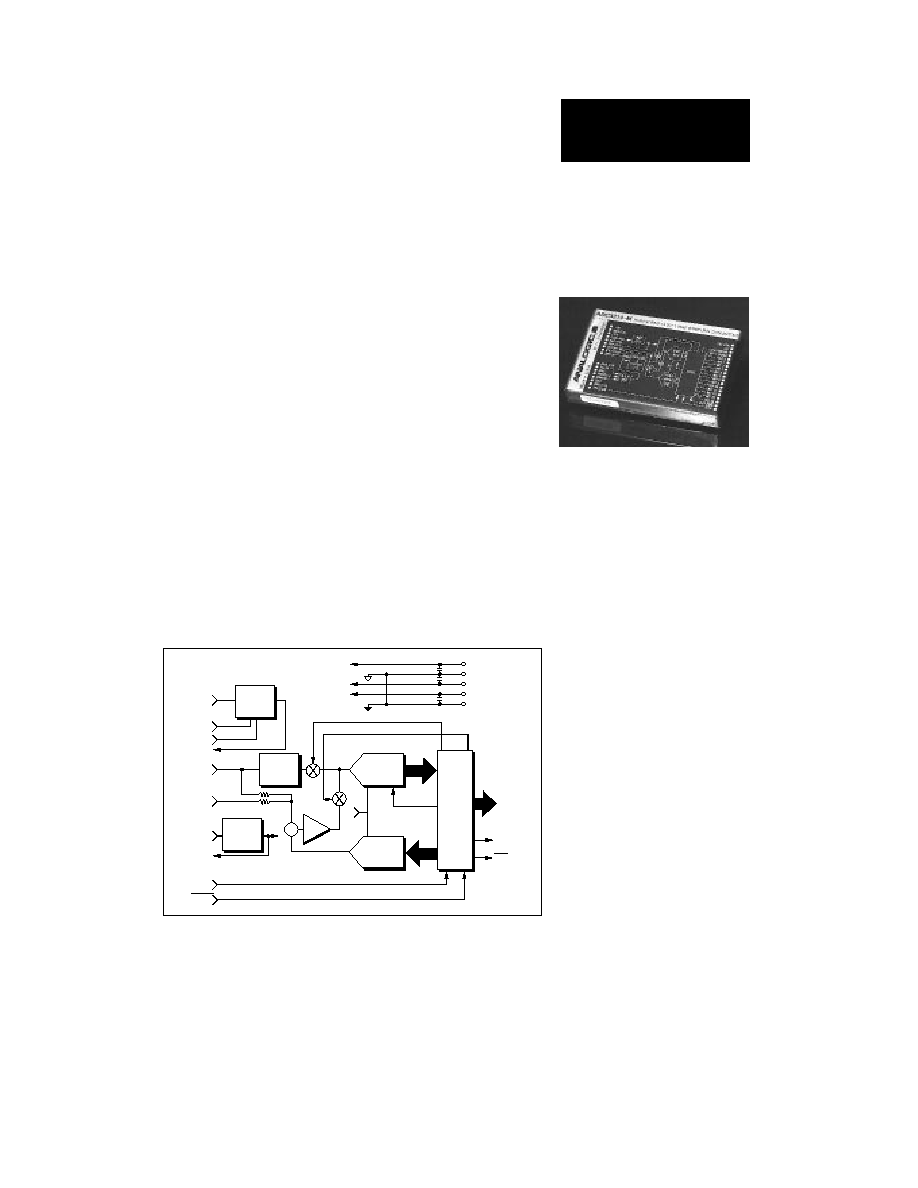
It is designed around a two-pass, subranging architecture that integrates
a low distortion sample-and-hold amplifier, precision voltage reference,
all the necessary timing circuitry and tri-state CMOS/TTL-compatible out-
puts for ease of system integration.
Features
u
14-Bit Resolution
u
1 MHz Throughput Rate
u
Reduced Cost
u
Reduced Size
u
No Missing Codes:
0∞C to +60∞C
u
Signal-to-Noise Ratio:
76 dB
u
Peak Distortion:
≠82 dB @ 100 kHz
u
Total Harmonic Distortion:
≠80 dB @ 100 kHz
u
Ease of Use
u
Built-In S/H Amplifier
u
TTL Compatibility
u
High Input Impedance
(100 M
)
Applications
u
Radar
u
Analytical Instrumentation
u
Spectroscopy
u
Digital Telecommunications
u
Automatic Test Equipment
u
High-Resolution Imaging
u
Medical Data Acquisition
u
Multiplexed Data Acquisition
Figure 1. ADC3214 Functional Block Diagram.
High Speed, 14-Bit, 1 MHz,
Sampling A/D Converter
With Built-in Sample-and-Hold Amplifier
ADC3214
B1-B14
O/U Flow
S/H
Amplifier
Scaling &
Offset
Circuit
Ref.
Ckt.
4-Bit
Linear
DAC
8-Bit
ADC
Signal In
Range 1
Range 2
S/H Out
A/D In
Ext. Off
Adj.
Ext. Gain
Adj.
+Ref. Out
Trigger
Enable
Ref.
Ref.
ADC Clk.
P2
P1
L
o
g
i
c
+15V
Ana. Rtn.
≠15V
+5V
Dig. Rtn.
EOC
Continued on page 3.

ANALOG INPUT
Input Range
±1.25V, ±2.5V
Input Bias Current
5 nA Max.
S/H Input Capacitance
10 pF Typ.
S/H Input Resistance
100 M
Min.
A/D Input Resistance
1.25 k
to Ground
DIGITAL INPUTS
Compatibility
CMOS, TTL
Logic Levels
Logic "0"
≠0.5V Min., 0.8V Max.
Logic "1"
2.0V Min., 5.5V Max.
Trigger
Negative Edge Triggered
Loading
1 TTL Load
Pulse Width
210 ns Min., 390 ns Max.
Output Enable
Active Low; B1-B14, O/U Flow
Propagation Delay
50 ns Max.
DIGITAL OUTPUTS
Maximum Output Drive
±2 mA Min.
Logic Levels
Logic "0"
0V Min., +0.4V Max.
Logic "1"
+3.5V Min., 5.0V Max.
Output Coding
Parallel Data, Offset Binary
EOC
Falling Edge, data valid 20 ns prior to
falling edge
Over/Under Flow
Active High; 1/2 code below FS
INTERNAL REFERENCE
Voltage
10.0V Typ.
Stability
±15 ppm/∞C Typ.
Available Current
2
1 mA Max.
DYNAMIC CHARACTERISTICS
Maximum Throughput Rate
1 MHz Min.
A/D Conversion Time
600 ns Max.
S/H Aperture Delay
10 ns Typ.
S/H Aperture Jitter
15 ps RMS Typ., 30 ps RMS Max.
S/H Feedthrough
3
≠84 dB Typ., ≠80 dB Max.
Full Power Bandwidth
1.5 MHz Min., 2.5 MHz Typ.
Small Signal Bandwidth
3.5 MHz Typ.
Signal to Noise Ratio
4
76 dB Min., 78 dB Typ.
Peak Distortion
5
10 kHz
≠86 dB Max., ≠95 dB Typ.
100 kHz
≠82 dB Max., ≠89 dB Typ.
540 kHz
≠76 dB Typ.
Total Harmonic Distortion
6
10 kHz
≠84 dB Max.
100 kHz
≠80 dB Max.
540 kHz
≠74 dB Typ.
Step Response
7
400 ns to ±0.01%
500 ns to ±0.006%
TRANSFER CHARACTERISTICS
Resolution
14 bits
Quantization Error
±0.5 LSB
Relative Accuracy
±0.006% FSR Max.
Differential Non-Linearity
±0.75 LSB @ 25∞C, ±1 LSB from 0∞C to
60∞C
Monotonicity
Guaranteed
No Missing Codes
Guaranteed from 0∞C to 60∞C
Offset Error
8
±5 mV Max.
Gain Error
8
±0.1% FSR Max.
Noise
9
180 µV RMS Typ., 266 µV RMS Max.
STABILITY (0∞C TO 60∞C)
Differential Non-Linearity
±1 ppm FSR/∞C Max.
Offset Voltage
±100 µV/∞C Max.
Gain
±25 ppm FSR/∞C Max.
Warm-Up Time
10 minutes
±15V Supply Rejection
±15 ppm FSR/% change Max.
Offset
±15 ppm FSR/% Change Max.
Gain
±15 ppm FSR/% Change Max.
+5V Supply Rejection
Offset
±60 ppm FSR/% Change Max.
Gain
±60 ppm FSR/% Change Max.
POWER REQUIREMENTS
10
±15V Supplies
14.25V Min., 15.75V Max.
+5V Supply
+4.75V Min., +5.25V Max.
+15V Current Drain
48 mA Typ.
≠15V Current Drain
63 mA Typ.
+5V Current Drain
132 mA Typ.
Power Consumption
2.35W Typ.
ENVIRONMENTAL & MECHANICAL
Temperature Range
Rated Performance
0∞C to 60∞C
Storage
≠25∞C to 75∞C
Relative Humidity (Non-condensing)
0 to 85% to 60∞C
Dimensions
1.99" x 2.99" x 0.44"
(50.5 x 75.9 x 11.2 mm)
Shielding
Electromagnetic 5 sides
Case Potential
Ground
ADC3214
Specifications
1
NOTES
1. Unless otherwise noted, all specifications apply at 25∞C
ambient with power supplies of ±15V and ±5V.
2. External Reference Load to remain stable during conver-
sion.
3. Measured with a full scale step input with a 20V/µs slew
rate.
4. Signal-to-noise ratio represents the ratio between the RMS
value of the signal and the total RMS noise below the
Nyquist rate. The total RMS noise is computed by: (1) sum-
ming the noise power in all frequency bins not correlated
with the test signal; (2) estimating the total noise power
contained in all harmonic frequency bins; and (3) comput-
ing the RMS noise from the sum of (1) and (2).
5. Peak distortion represents the ratio between the highest
spurious frequency component below the Nyquist rate and
the signal. Note that in computing peak distortion the esti-
mated noise allocated to the harmonic frequency bins in
computing SNR is first removed. See Note 4.
6. Total harmonic distortion represents the ratio between the
RMS sum of all harmonics up to the 100th harmonic and
the RMS value of the signal. Note that in computing total
harmonic distortion, the estimated noise allocated to the
harmonic frequency bins in computing SNR is first re-
moved. See Note 4.
7. Step Response represents the time required to achieve the
specified accuracies after a full scale step change at the
signal input, specified at a 1 MHz throughput rate.
8. Externally adjustable to zero. See coding and trim proce-
dure.
9. Thermal noise from the S/H and A/D converter, not includ-
ing quantization noise.
10. Analogic highly recommends the use of linear power sup-
plies with its high performance, high resolution A/D con-
verters. However, if system requirements provide only a
+5V supply and limited space, the use of the Analogic
SP7015 DC-to-DC converter will provide a low noise solu-
tion which will not degrade the ADC3214 performance.
Specifications subject to change without notice.
Superior performance and ease-of-use make the
ADC3214 the ideal solution for applications requiring a
sample-and-hold amplifier directly at the input to the A/D
converter. Having the S/H amplifier integrated with the
A/D converter benefits the system designer in two ways.
First, the S/H has been designed specifically to comple-
ment the performance of the A/D converter; for exam-
ple, the acquisition time, hold mode settling and droop
rate have been optimized for the A/D converter, resulting
in exceptional overall performance. Second, the design-
er achieves true 14-bit performance, avoiding degrada-
tion due to ground loops, signal coupling, jitter and digi-
tal noise introduced when separate S/H and A/D con-
vertesr are interconnected. Furthermore, the accuracy,
speed, and quality of the ADC3214 are fully ensured by
thorough, computer-controlled factory tests of each unit.
ADC3214 SPECIFICATIONS
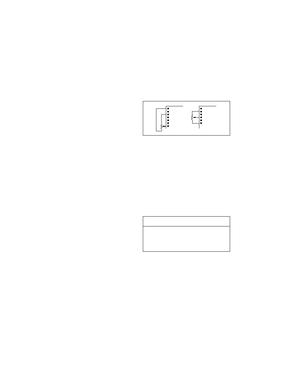
Coding and Trim Procedure
Refer to Figures 2 and 3 for the ADC3214 Coding and
Trim Procedure. Figure 2 shows the external Offset and
Gain Adjust configuration. Figure 3 shows the output
Offset Binary coding of the ADC3214 A/D converter.
The voltages mentioned in the following Trim
Procedure refer to the ±2.5V input range with the num-
bers in parentheses referring to the ±1.25V input range.
To trim the offset of the ADC3214, apply ≠153 µV (≠76
µV) to the analog input. Adjust the external offset trim
potentiometer such that each of the 14 bits alternates
equally between "0" and "1". Using the setup as de-
scribed in Figure 2, the sensitivity of the offset adjust-
ment is typically 6 LSBs per volt.
To trim the gain of the ADC3214, apply +2.499542V
(+1.249771V) to the analog input and adjust the exter-
nal gain trim potentiometer such that the 13 MSBs are
"1" and the LSB alternates equally between "0" and "1".
Using the setup as described in Figure 2, the sensitivi-
ty of the gain adjustment is typically 0.14% per volt.
Timing Considerations
The timing diagram in Figure 4 shows the timing char-
acteristics of the ADC3214 A/D converter. Upon a
high-to-low transition of the Trigger input, the internal
logic of the ADC3214 places the input S/H amplifier
(see Figure 1) into the Hold mode. Approximately 550
ns after Trigger, the internal S/H amplifier returns to the
Sample mode to begin acquiring the next sample.
Offset Adjustment
Gain Adjustment
≠15V
+15V
Ext. Off. Adj.
1
3
7
50 k
Ana. Rtn.
Ext. Gain Adj.
+Ref. Out
2
4
6
10 k
Figure 2. External Offset and Gain Adjust
Configuration.
ANALOG INPUT
DIGITAL OUTPUT ±1.25V ±2.5V
MSB
LSB
1 1 1 1 1 1 1 1 1 1 1 1 1 1
= +1.24985V +2.49970V
1 0 0 0 0 0 0 0 0 0 0 0 0 0
= 0.00000V
0.00000V
0 0 0 0 0 0 0 0 0 0 0 0 0 0
= 1.25000V ≠2.50000V
B1,B2
. . . . .B14
= Pin Label
Figure 3. Output Coding for the ADC3214.
Continued from page 1.
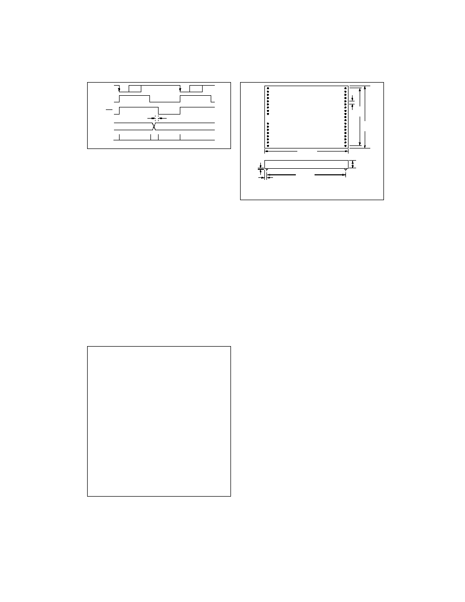
Approximately 200 ns later (750 ns elapsed time), the
A/D converter has completed the conversion process
and latches the data into the output tri-state latches.
The data is valid 20 ns prior to the high-to-low transi-
tion of the EOC pulse.
Layout Considerations
The high resolution of the ADC3214 A/D converter
makes it necessary to pay careful attention to the print-
ed circuit layout for the device. It is, for example, im-
portant to separate analog and digital grounds and to
return them separately to the system power supply.
Digital grounds are often noisy or "glitchy," and these
glitches can have adverse effects on the performance
of the ADC3214 if they are introduced to the analog
portions of the A/D converter's circuitry. At 14-bit reso-
lution, the size of the voltage step between one code
transition and the succeeding one is only 152 µV (305
µV for the ±2.5V range), so it is evident that any noise
in the analog ground return can result in erroneous or
missing codes. It is therefore important to configure a
low-impedance ground-plane return on the printed-cir-
cuit board. This is the point where the analog and
digital returns should be made common, NOT at the
supplies.
PRINCIPLES OF OPERATION
To understand the operating principles of the ADC3214
A/D converter, refer to Figures 4 and 7. The simplified
block diagram of Figure 7 illustrates the two succes-
sive passes in the sub-ranging conversion scheme of
the ADC3214.
The ADC3214 is a 14-bit sampling A/D converter with
throughput rates to 1 MHz. It has two externally config-
urable input ranges of ±1.25V and ±2.5V. This is easily
accomplished by externally connecting Pins 15 and 16
for the ±1.25V range and leaving both pins open (N/C)
for the ±2.5 range (see Figure 5). The S/H amplifier
has a gain of X≠1 or X≠2, providing an output of ±2.5V
regardless of the input. This simplifies the calibration of
the ADC by reducing the required gain of the summing
amplifier.
The first pass starts at a high-to-low transition of the
trigger pulse. This signal places the S/H into the Hold
mode and starts the timing logic. In the first pass, the
output of the S/H is attenuated by a factor of 0.4 and
offset to convert the 5V full scale ADC range to the 2V
full scale range of the flash ADC. After approximately
110 ns, the attenuator circuitry has settled to 9-bit ac-
curacy at which time the ADC digitizes the first pass.
The 8 bits take two paths: to the internal logic and to
the 8 most significant bits of a 14-bit accurate D/A con-
verter, setting up the second pass.
1. ≠15V
38.
DIG
RTN
2.
ANA RTN
37.
+5V
3.
+15V
36.
O/U RANGE
4.
EXT RANGE ADJ
35.
BIT 1 (MSB)
5.
REF RTN
34.
BIT 2
6.
+V REF OUT
33.
BIT 3
7.
EXT OFFS ADJ
32.
BIT 4
8.
S/H ANA OUT
31.
BIT 5
9.
ADC IN
31.
BIT 6
10.
NO PIN
29.
BIT 7
11.
NO PIN
28.
BIT 8
12.
ANA RTN
27.
BIT 9
13.
SIGNAL IN
26.
BIT 10
14.
DO NOT CONNECT
25.
BIT 11
15.
RANGE 2
24.
BIT 12
16.
RANGE 1
23.
BIT 13
17.
DO NOT CONNECT
22.
BIT 14
18.
ANA RTN
21.
OUT ENABLE
19.
TRIGGER
20. EOC
CONNECT PIN 8 TO PIN 9.
Figure 5. ADC3214 Pin Assignments.
0.100"
Top View
1.800"
Typ.
1.990"
Max.
2.990" Max.
2.800" Typ.
0.015"
Min.
0.095"
Max.
0.095" Max.
0.440"
Max.
Side View
Recommended Hole Size: 0.035
Pin Diameter: 0.020 Typical
Pin Length: 0.125" to 0.250"
1
38
19
20
Figure 6. ADC3214 Mechanical.
N
N+1
20 ns
N
N≠1
0
550 750
1000
Trigger
S/H Cont.
(Int.)
Data Valid
Timing (ns)
EOC
Figure 4. ADC3214 Timing Diagram.
In the second pass, the output of the D/A converter is
subtracted from the output of the S/H amplifier. The
nominal error voltage of ±0.5 LSB (at the 8-bit level it is
5V/256 or 19.5 mV) is amplified by 25.6 to achieve 1/4
full scale range of the flash ADC, thus allowing a 2-bit
overlap safety margin. The effective resolution there-
fore becomes the digital summation of two 8-bit results
with the 2 LSBs of Pass 1 overlapping the 2 MSBs of
Pass 2. At approximately 550 ns after trigger, the error
signal has settled to 14-bit accuracy and the ADC then
digitizes the second pass. The internal logic then
places the S/H back into the Sample mode to begin
acquiring the next sample. The second pass data is
latched into the output tri-state registers and the con-
version is now complete. This is marked by a high-to-
low transition of the EOC pulse with the data valid 20
ns prior to EOC.
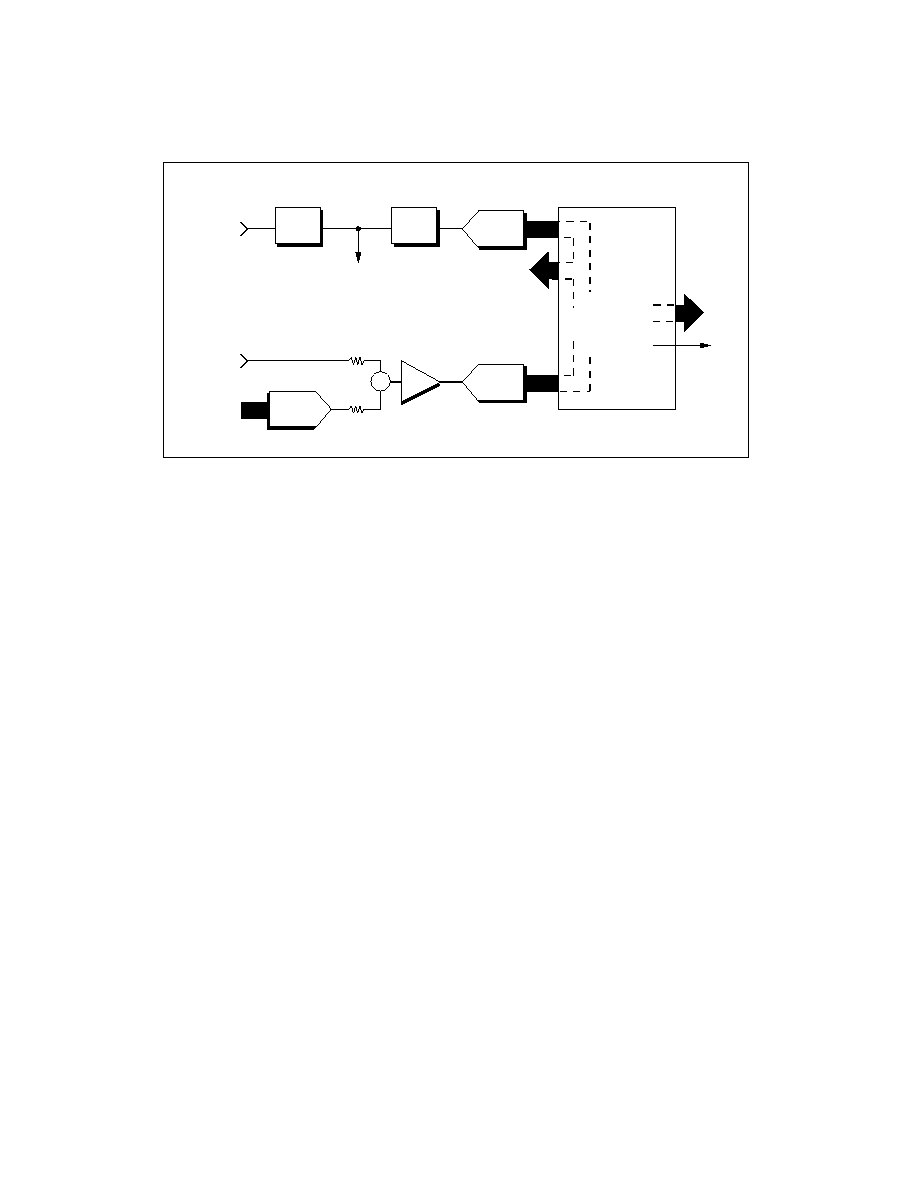
The ADC3214 has a tri-state output structure. Users
can enable the fourteen data bits and the
Overflow/Underflow bit with the ENABLE pin. This fea-
ture makes it possible to transfer data from the
ADC3214 to a microprocessor bus. However, to pre-
vent the coupling of high frequency noise from the mi-
croprocessor bus into the A/D converter, the output
data must be buffered (see Figure 8).
The 1/4 full scale range, or 2-bit overlap in the second
pass, is a scheme used in the ADC3214 to provide an
output word that is accurate and linear to 14 bits. This
method corrects for gain and linearity errors in the am-
plifying circuitry, as well as the 8-bit flash A/D convert-
er. Without the use of this overlapping correction
scheme, it would be necessary that all the components
in the ADC3214 be accurate to the 14-bit level. While
such a design might be possible to realize on a labora-
tory benchtop, it clearly would be impractical to
achieve on a production basis. The key to the conver-
sion technique used in the ADC3214 is the 14-bit ac-
curate and 14-bit linear D/A converter, which serves as
the reference element for the conversion's second
pass. The use of proprietary sub-ranging architecture
in the ADC3214 results in a sampling A/D converter
that offers unprecedented speed and transfer charac-
teristics at the 14-bit level.
8-Bit
ADC
Analog
Input
S/H
Amplifier
Scaling &
Offset Circuit
x0.4
Overlap
Logic
8-Bit
ADC
To Summing Amp
for 2nd Pass
2V p-p
1st Pass
From
S/H Out
2nd Pass
X25.6
0.5V p-p
14-Bit
Linear
DAC
Logic
B1-B14
O/U
8 MSBs
From 1st
Pass
Logic
To 14-Bit DAC
for 2nd Pass
Figure 7. Simplified Block Diagram.