General Description
The MAX9705 3rd-generation, ultra-low EMI, mono, Class
D audio power amplifier provides Class AB performance
with Class D efficiency. The MAX9705 delivers 2.3W into
a 4
load and offers efficiencies above 85%. Active
emissions limiting (AEL) circuitry greatly reduces EMI by
actively controlling the output FET gate transitions under
all possible transient output-voltage conditions. AEL pre-
vents high-frequency emissions resulting from conven-
tional Class D free-wheeling behavior in the presence of
an inductive load. Zero dead time (ZDT) technology
maintains state-of-the-art efficiency and THD+N perfor-
mance by allowing the output FETs to switch simultane-
ously without cross-conduction. A patented spread-
spectrum modulation scheme eliminates the need for out-
put filtering found in traditional Class D devices. These
design concepts reduce an application's component
count and extend battery life.
The MAX9705 offers two modulation schemes: a fixed-
frequency (FFM) mode and a spread-spectrum (SSM)
mode that further reduces EMI-radiated emissions due to
the modulation frequency. The MAX9705 oscillator can
be synchronized to an external clock through the SYNC
input, allowing the switching frequency to be externally
defined. The SYNC input also allows multiple MAX9705s
to be cascaded and frequency locked, minimizing inter-
ference due to clock intermodulation. The device utilizes
a fully differential architecture, a full-bridged output, and
comprehensive click-and-pop suppression. The gain of
the MAX9705 is set internally (MAX9705A: 6dB,
MAX9705B: 12dB, MAX9705C: 15.6dB, MAX9705D:
20dB), further reducing external component count.
The MAX9705 is available in 10-pin TDFN (3mm x 3mm x
0.8mm), 10-pin �MAX
�
, and 12-bump UCSPTM (1.5mm x
2mm x 0.6mm) packages. The MAX9705 is specified over
the extended -40�C to +85�C temperature range.
Applications
Features
Filterless Amplifier Passes FCC-Radiated
Emissions Standards with 24in of Cable
Unique Spread-Spectrum Mode and Active
Emissions Limiting (AEL) Achieves Better than
20dB Margin Under FCC Limits
Zero Dead Time (ZDT) H-Bridge Maintains State-
of-the-Art Efficiency and THD+N
Simple Master-Slave Setup for Stereo Operation
Up to 90% Efficiency
2.3W into 4 (1% THD+N)
Low 0.02% THD+N (P
OUT
= 1W, V
DD
= 5.0V)
High PSRR (75dB at 217Hz)
Integrated Click-and-Pop Suppression
Low Quiescent Current (5.4mA)
Low-Power Shutdown Mode (0.3�A)
Short-Circuit and Thermal-Overload Protection
Available in Thermally Efficient, Space-Saving
Packages
10-Pin TDFN (3mm x 3mm x 0.8mm)
10-Pin �MAX
12-Bump UCSP (1.5mm x 2mm x 0.6mm)
Pin-for-Pin Compatible with the MAX9700 and
MAX9712
MAX9705
2.3W, Ultra-Low-EMI, Filterless,
Class D Audio Amplifier
________________________________________________________________ Maxim Integrated Products
1
Ordering Information
19-3405; Rev 0; 7/05
For pricing, delivery, and ordering information, please contact Maxim/Dallas Direct! at
1-888-629-4642, or visit Maxim's website at www.maxim-ic.com.
EVALUATION KIT
AVAILABLE
Cellular Phones
PDAs
MP3 Players
Portable Audio
PART
TEMP RANGE
PIN-
PACKAGE
TOP
MARK
MAX9705AETB+T
-40
o
C to +85
o
C
10 TDFN-10
ACY
MAX9705AEUB+
-40
o
C to +85
o
C
10 �MAX
--
MAX9705AEBC+T
-40
o
C to +85
o
C
12 UCSP-12
ACH
MAX9705BETB+T
-40
o
C to +85
o
C
10 TDFN-10
ACX
MAX9705BEUB+
-40
o
C to +85
o
C
10 �MAX
--
MAX9705BEBC+T
-40
o
C to +85
o
C
12 UCSP-12
ACG
Ordering Information continued at end of data sheet.
�MAX is a registered trademark and UCSP is a trademark of
Maxim Integrated Products, Inc.
+Denotes lead-free package.
Selector Guide appears at end of data sheet.
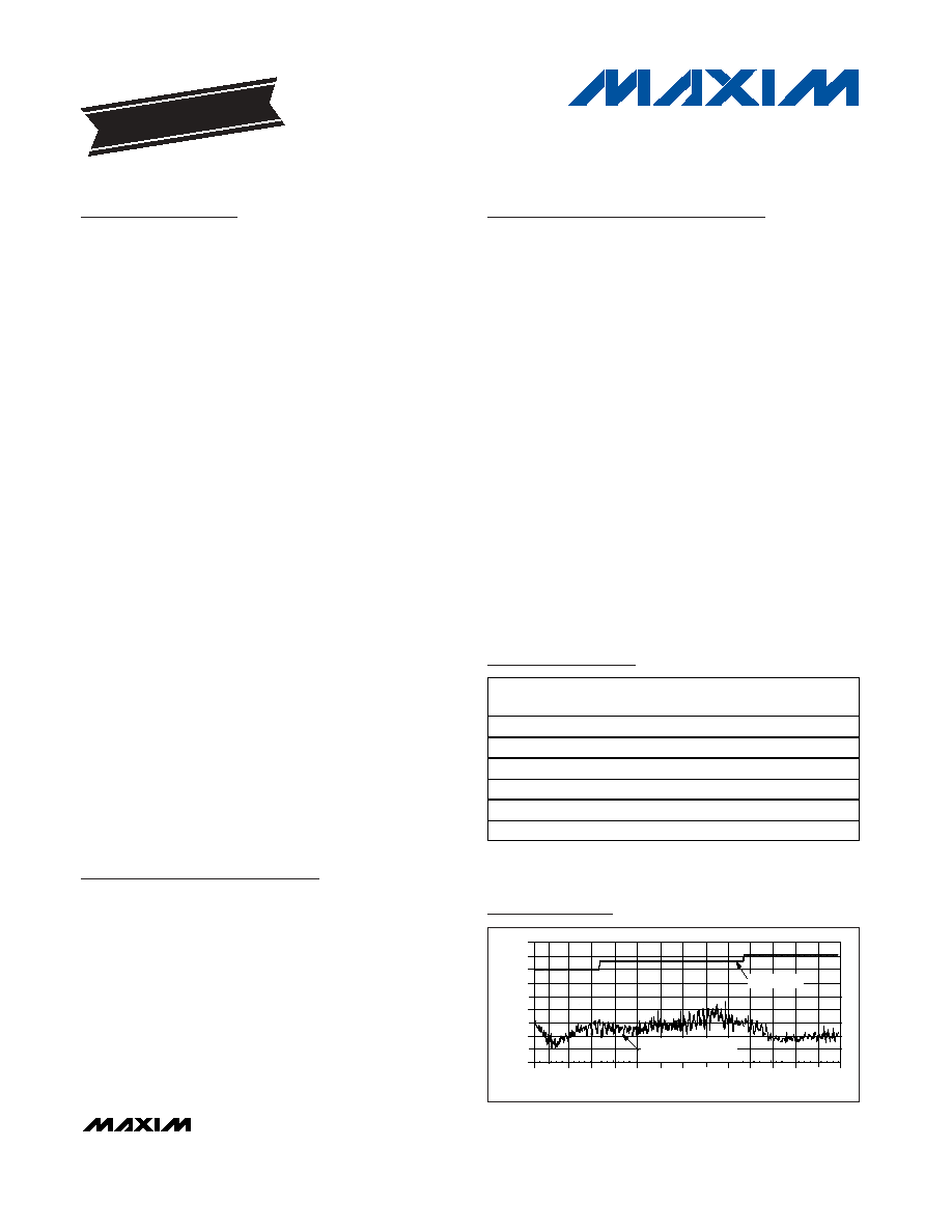
30.0
60.0 80.0 100.0 120.0 140.0 160.0 180.0 200.0 220.0 240.0 260.0 280.0 300.0
5.0
10.0
15.0
20.0
25.0
30.0
35.0
40.0
45.0
50.0
FREQUENCY (MHz)
AMPLITUDE (dB
�
V/m)
FCC EMI LIMIT
MAXIM'S NEW ULTRA-LOW
OUTPUT SPECTRUM
EMI Spectrum Diagram

2.3W, Ultra-Low-EMI, Filterless,
Class D Audio Amplifier
2
_______________________________________________________________________________________
ABSOLUTE MAXIMUM RATINGS
ELECTRICAL CHARACTERISTICS
(V
DD
= PV
DD
=
SHDN = 3.3V, GND = PGND = 0V, SYNC = GND (FFM), R
L
=
, R
L
connected between OUT+ and OUT-, T
A
= T
MIN
to T
MAX
, unless otherwise noted. Typical values are at T
A
= +25�C.) (Notes 1, 2)
Stresses beyond those listed under "Absolute Maximum Ratings" may cause permanent damage to the device. These are stress ratings only, and functional
operation of the device at these or any other conditions beyond those indicated in the operational sections of the specifications is not implied. Exposure to
absolute maximum rating conditions for extended periods may affect device reliability.
V
DD
to GND..............................................................................6V
PV
DD
to PGND .........................................................................6V
GND to PGND .......................................................-0.3V to +0.3V
PV
DD
to V
DD
..........................................................-0.3V to +0.3V
All Other Pins to GND.................................-0.3V to (V
DD
+ 0.3V)
Continuous Current Into/Out of PV
DD
/PGND/OUT_........�600mA
Continuous Input Current (all other pins) .........................�20mA
Duration of OUT_ Short Circuit to GND or PV
DD
........Continuous
Duration of Short Circuit Between OUT+ and OUT-.....Continuous
Continuous Power Dissipation (T
A
= +70�C)
10-Pin TDFN (derate 24.4mW/�C above +70�C) .....1951.2mW
10-Pin �MAX (derate 5.6mW/
o
C above +70�C) .........444.4mW
12-Bump UCSP (derate 6.1mW/�C above +70�C)........484mW
Junction Temperature ......................................................+150�C
Operating Temperature Range ...........................-40�C to +85�C
Storage Temperature Range .............................-65�C to +150�C
Lead Temperature (soldering, 10s) .................................+300�C
Bump Temperature (soldering)
Reflow ..........................................................................+235�C
MAX9705
PARAMETER
SYMBOL
CONDITIONS
MIN
TYP
MAX
UNITS
GENERAL
Supply Voltage Range
V
DD
Inferred from PSRR test
2.5
5.5
V
Quiescent Current
I
DD
5.4
7
mA
Shutdown Current
I
SHDN
0.3
10
�A
Turn-On Time
t
ON
30
ms
Input Resistance
R
IN
T
A
= +25�C
12
20
k
MAX9705A
0.88
1.0
1.12
MAX9705B
0.73
0.83
0.93
MAX9705C
0.61
0.71
0.81
Input Bias Voltage
V
BIAS
Either input
MAX9705D
0.48
0.56
0.64
V
MAX9705A
1.9
2.0
2.1
MAX9705B
3.8
4.0
4.2
MAX9705C
5.7
6.0
6.3
Voltage Gain
A
V
MAX9705D
9.5
10
10.5
V/V
Output Offset Voltage
V
OS
T
A
= +25�C
�10
�69
mV
Common-Mode Rejection Ratio
CMRR
f
IN
= 1kHz, input referred
56
dB
V
DD
= 2.5V to 5.5V, T
A
= +25�C
50
75
f
RIPPLE
= 217Hz
75
Power-Supply Rejection Ratio
(Note 3)
PSRR
200mV
P-P
ripple
f
RIPPLE
= 20kHz
60
dB
R
L
= 8
600
Output Power
P
OUT
THD+N = 1%,
f
IN
= 1kHz
R
L
= 4
950
mW
R
L
= 8
,
P
OUT
= 450mW
0.02
Total Harmonic Distortion
Plus Noise
THD+N
f
IN
= 1kHz, either FFM or
SSM
R
L
= 4
,
P
OUT
= 375mW
0.025
%
Into shutdown
-68
Click/Pop Level
K
CP
Peak voltage,
A-weighted (Notes 3, 4)
Out of shutdown
-60.5
dB
MAX9705
2.3W, Ultra-Low-EMI, Filterless,
Class D Audio Amplifier
_______________________________________________________________________________________
3
ELECTRICAL CHARACTERISTICS (continued)
(V
DD
= PV
DD
=
SHDN = 3.3V, GND = PGND = 0V, SYNC = GND (FFM), R
L
=
, R
L
connected between OUT+ and OUT-, T
A
= T
MIN
to T
MAX
, unless otherwise noted. Typical values are at T
A
= +25�C.) (Notes 1, 2)
Note 1: All devices are 100% production tested at +25�C. All temperature limits are guaranteed by design.
Note 2: Testing performed with a resistive load in series with an inductor to simulate an actual speaker load. For R
L
= 4
, L = 33�H.
For R
L
= 8
, L = 68�H. For R
L
= 16
, L = 136�H.
Note 3: Inputs AC-coupled to GND.
Note 4: Testing performed with 8
resistive load in series with 68�H inductive load connected across BTL output. Mode transitions
are controlled by
SHDN pin. K
CP
level is calculated as 20 x log[(peak voltage under normal operation at rated power
level)/(peak voltage during mode transition, no input signal)]. Units are expressed in dB.
Note 5: SYNC has a 1M
resistor to V
REF
= 1.25V.
PARAMETER
SYMBOL
CONDITIONS
MIN
TYP
MAX
UNITS
Output Slew Rate
SR
176
V/�s
Rise/Fall Time
t
RISE
, t
FALL
10% to 90%
15
ns
FFM
91
BW = 22Hz
to 22kHz
SSM
89
FFM
93
Signal-to-Noise Ratio
SNR
V
OUT
= 2V
RMS
A-weighted
SSM
91
dB
SYNC = GND
980
1100
1220
SYNC = float
1250
1450
1650
Oscillator Frequency
f
OSC
SYNC = V
DD
(SSM mode)
1220
�120
kHz
SYNC Frequency Lock Range
800
2000
kHz
Efficiency
P
OUT
= 800mW, f
IN
= 1kHz, R
L
= 8
89
%
DIGITAL INPUTS (
SHDN, SYNC)
V
IH
2
Input Thresholds
V
IL
0.8
V
SHDN Input Leakage Current
0.1
�10
�A
SYNC Input Current
(Note 5)
-1.25
�10
�A
ELECTRICAL CHARACTERISTICS
(V
DD
= PV
DD
=
SHDN = 5V, GND = PGND = 0V, SYNC = GND (FFM), R
L
=
, R
L
connected between OUT+ and OUT-, T
A
= T
MIN
to
T
MAX
, unless otherwise noted. Typical values are at T
A
= +25�C.) (Notes 1, 2)
PARAMETER
SYMBOL
CONDITIONS
MIN
TYP
MAX
UNITS
Quiescent Current
I
DD
7
mA
Shutdown Current
I
SHDN
0.55
�A
f = 217Hz
75
Power-Supply Rejection Ratio
PSRR
200mV
P-P
ripple
f = 20kHz
60
dB
R
L
= 16
750
R
L
= 8
1400
Output Power
P
OUT
THD+N = 1%,
f = 1kHz
R
L
= 4
2300
mW
R
L
= 8
, P
OUT
= 1.0W
0.02
Total Harmonic Distortion
Plus Noise
THD+N
f = 1kHz, either
FFM or SSM
R
L
= 4
, P
OUT
= 1.75W
0.05
%
FFM
94
BW = 22Hz to
22kHz
SSM
91
FFM
97
Signal-to-Noise Ratio
SNR
V
OUT
=
3V
RMS
A-weighted
SSM
93
dB
100
0
0.5
1.0
1.5
10
1
0.1
0.01
0.001
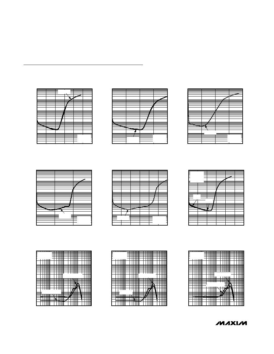
TOTAL HARMONIC DISTORTION
PLUS NOISE vs. OUTPUT POWER
MAX9705toc04
OUTPUT POWER (W)
THD+N (%)
V
DD
= 3.3V
R
L
= 4
f
IN
= 1kHz
100
0
1.0
0.5
2.0
1.5
2.5
3.0
10
1
0.1
0.01
0.001
TOTAL HARMONIC DISTORTION
PLUS NOISE vs. OUTPUT POWER
MAX9705toc05
OUTPUT POWER (W)
THD+N (%)
f
IN
= 1kHz
V
DD
= 5.0V
R
L
= 4
100
0
0.4
0.2
0.8
0.6
1.0
1.2
10
1
0.1
0.01
0.001
TOTAL HARMONIC DISTORTION
PLUS NOISE vs. OUTPUT POWER
MAX9705toc06
OUTPUT POWER (W)
THD+N (%)
V
DD
= 3.3V
R
L
= 8
f
IN
= 1kHz
FFM
SSM
100
0.01
10
100
10k
100k
TOTAL HARMONIC DISTORTION
PLUS NOISE vs. FREQUENCY
0.1
1
10
MAX9705toc07
FREQUENCY (Hz)
THD+N (%)
1k
V
DD
= 3.3V
R
L
= 8
P
OUT
= 100mW
P
OUT
= 450mW
100
0.01
10
100
10k
100k
TOTAL HARMONIC DISTORTION
PLUS NOISE vs. FREQUENCY
0.1
1
10
MAX9705toc08
FREQUENCY (Hz)
THD+N (%)
1k
V
DD
= 5.0V
R
L
= 8
P
OUT
= 250mW
P
OUT
= 1W
100
0.01
10
100
10k
100k
TOTAL HARMONIC DISTORTION
PLUS NOISE vs. FREQUENCY
0.1
1
10
MAX9705toc09
FREQUENCY (Hz)
THD+N (%)
1k
V
DD
= 2.5V
R
L
= 4
P
OUT
= 50mW
P
OUT
= 300mW
MAX9705
2.3W, Ultra-Low-EMI, Filterless,
Class D Audio Amplifier
4
_______________________________________________________________________________________
Typical Operating Characteristics
(V
DD
= 3.3V, SYNC = V
DD
(SSM), differential input, T
A
= +25�C, unless otherwise noted.)
100
0
0.4
0.8
1.0
0.2
0.6
1.2
10
1
0.1
0.01
0.001
TOTAL HARMONIC DISTORTION
PLUS NOISE vs. OUTPUT POWER
MAX9705toc01
OUTPUT POWER (W)
THD+N (%)
f
IN
= 1kHz
V
DD
= 3.3V
R
L
= 8
100
0
0.5
1.0
1.5
2.0
10
1
0.1
0.01
0.001
TOTAL HARMONIC DISTORTION
PLUS NOISE vs. OUTPUT POWER
MAX9705toc02
OUTPUT POWER (W)
THD+N (%)
f
IN
= 1kHz
V
DD
= 5.0V
R
L
= 8
100
0
0.2
0.4
0.6
0.8
10
1
0.1
0.01
0.001
TOTAL HARMONIC DISTORTION
PLUS NOISE vs. OUTPUT POWER
MAX9705toc03
OUTPUT POWER (W)
THD+N (%)
f
IN
= 1kHz
V
DD
= 2.5V
R
L
= 4

MAX9705
2.3W, Ultra-Low-EMI, Filterless,
Class D Audio Amplifier
_______________________________________________________________________________________
5
Typical Operating Characteristics (continued)
(V
DD
= 3.3V, SYNC = V
DD
(SSM), differential input, T
A
= +25�C, unless otherwise noted.)
100
0.01
10
100
10k
100k
TOTAL HARMONIC DISTORTION
PLUS NOISE vs. FREQUENCY
0.1
1
10
MAX9705toc10
FREQUENCY (Hz)
THD+N (%)
1k
V
DD
= 3.3V
R
L
= 4
P
OUT
= 100mW
P
OUT
= 800mW
100
0.01
10
100
10k
100k
TOTAL HARMONIC DISTORTION
PLUS NOISE vs. FREQUENCY
0.1
1
10
MAX9705toc11
FREQUENCY (Hz)
THD+N (%)
1k
V
DD
= 5.0V
R
L
= 4
P
OUT
= 250mW
P
OUT
= 1.75W
100
0.01
10
100
10k
100k
TOTAL HARMONIC DISTORTION
PLUS NOISE vs. FREQUENCY
0.1
1
10
MAX9705toc12
FREQUENCY (Hz)
THD+N (%)
1k
V
DD
= 3.3V
R
L
= 8
P
OUT
= 450mW
FFM
SSM
100
0
0.5
1.5
1.0
2.0
2.5
10
1
0.1
0.01
0.001
TOTAL HARMONIC DISTORTION PLUS
NOISE vs. COMMON-MODE VOLTAGE
MAX9705toc13
COMMON-MODE VOLTAGE (V)
THD+N (%)
V
DD
= 3.3V to 5V
f
IN
= 1kHz
P
OUT
= 500mW
GAIN = 6dB
R
L
= 8
0
30
20
10
40
50
60
70
80
90
100
0
0.4
0.2
0.6
0.8
1.0
EFFICIENCY
vs. OUTPUT POWER
MAX9705toc14
OUTPUT POWER (W)
EFFICIENCY (%)
V
DD
= 3.3V
f
IN
= 1kHz
R
L
= 8
R
L
= 4
0
30
20
10
40
50
60
70
80
90
100
0
1.0
0.5
1.5
2.0
2.5
3.0
EFFICIENCY
vs. OUTPUT POWER
MAX9705toc15
OUTPUT POWER (W)
EFFICIENCY (%)
V
DD
= 5.0V
f
IN
= 1kHz
R
L
= 8
R
L
= 4
0
30
20
10
40
50
60
70
80
90
100
2.5
3.5
3.0
4.0
4.5
5.0
5.5
EFFICIENCY
vs. SUPPLY VOLTAGE
MAX9705toc16
SUPPLY VOLTAGE (V)
EFFICIENCY (%)
f
IN
= 1kHz
THD+N = 1%
R
L
= 8
R
L
= 4
0
30
20
10
40
50
60
70
80
90
100
800
1200
1000
1400
1600
1800
2000
EFFICIENCY
vs. SYNC FREQUENCY
MAX9705toc17
SYNC FREQUENCY (kHz)
EFFICIENCY (%)
V
DD
= 3.3V
f
IN
= 1kHz
THD+N = 1%
R
L
= 8
R
L
= 4
0
30
20
10
40
50
60
70
80
90
100
800
1200
1000
1400
1600
1800
2000
EFFICIENCY
vs. SYNC FREQUENCY
MAX9705toc18
SYNC FREQUENCY (kHz)
EFFICIENCY (%)
V
DD
= 5.0V
f
IN
= 1kHz
THD+N = 1%
R
L
= 8
R
L
= 4