
Replacement of
LM2575 Series
MIK2575 Series
Simple Switcher (1A Step-
Down Voltage Regulator)
October 2001 - revised July 2002
Description
The MIK2575 series of regulators are monolithic integrated circuits that provide all the active functions for a step-down (buck) switching
regulator, capable of driving 1A load with excellent line and load regulation. Requiring a minimum number of external components,
these regulators are simple to use and include internal frequency compensation and a fixed-frequency oscillator. The MIK2575 series
offers a high-efficiency replacement for popular three-terminal linear regulators. It substantially reduces the size of the heat sink, and in
some cases no heat sink is required. Other features include a guaranteed
± 4% tolerance on output voltage within specified input
voltages and output load conditions, and
±10% on the oscillator frequency The output switch includes cycle-by-cycle current limiting, as
well as thermal shutdown for full protection under fault conditions.
Features
3.3V, 5V, 12V, 15V, and adjustable output versions
Adjustable version output voltage range, 1.23V to 37V
± 4%
max over line and load conditions
Guaranteed 1A output current
Wide input voltage range
Requires only 4 external components
52 kHz fixed frequency oscillator
TTL shutdown capability, low power standby mode
Uses readily available standard inductors
Thermal shutdown and current limit protection
Applications
Simple high-efficiency step-down (buck) regulator
Efficient pre-regulator for linear regulators
On-card switching regulators
Positive to negative converter (Buck-Boost)
Typical application
(Fixed Output Voltage Versions)
7V - 40V
UNREGULATED
DC INPUT
MIK2575-5.0
+V
IN
+5V, 1A
REGULATED
OUTPUT
1
+
C
IN
3
GND
ON/OFF
OUTPUT
4
L1
330 H
D1
1N5819
C
OUT
330 F
100 F
FEEDBACK
5
+
2
Note: Pin numbers are for the TO-220 package.
Block Diagram
+
C
IN
C
OUT
FEED-
BACK
+
1
4
+
-
-
+
DRIVER
1.23V
BAND-GAP
REFERENCE
52kHZ
OSCILLATOR
RESET
THERMAL
SHUTDOWN
CURRENT
LIMIT
3
2
L1
INTERNAL
REGULATOR
ON/OFF
5
R2
R1
1.0k
FIXED GAIN
ERROR AMP
COMPARATOR
3 AMP
SWITCH
OUTPUT
GND
V
OUT
D1
ON/OFF
V
IN
UNREGULATED
DC INPUT
Note: Pin numbers are for the TO-220 package.
Page 1 of 5
Replacement of
LM2575 Series
MIK2575 Series
Simple Switcher (1A Step-
Down Voltage Regulator)
October 2001 - revised July 2002
Absolute Maximum Ratings
(unless otherwise noted)
Parameter Maximum
Units
Maximum Supply Voltage
45
ON/OFF Pin Input Voltage
-0.3V
V +V
IN
V
Input Voltage to Ground
-1 V
Power Dissipation
Internally Limited
W
Storage Temperature Range
-65 to +150
°C
Maximum Junction Temperature
150
°C
Lead Temperature (Soldering, 10 Seconds)
260
°C
Operating Ratings
Parameter Value
Units
Temperature Range
-40
T
J
+125
°C
Supply Voltage
40 V
Electrical Characteristics
(T
J
= 25
°C, unless otherwise noted) Note 1
Symbol Parameter
Conditions
Min
Typ
Max
Units
Output Voltage
MIK2575-3.3 V
IN
=12V, I
LOAD
=0.2A Circuit of Figure 1
3.234 3.366
V
OUT
4.75V
V
IN
40V, 0.2A I
LOAD
1A;
Circuit of Figure 1
* 3.168
3.135
3.3
3.432
3.465
MIK2575-5.0 V
IN
=12V, I
LOAD
=0.2A Circuit of Figure 1
4.900
5.100
8V
V
IN
40V, 0.2A I
LOAD
1A
Circuit of Figure 1
*
4.800
4.750
5.0
5.200
5.250
MIK2575-12 V
IN
=25 V, I
LOAD
=0.2A Circuit of Figure 1
11.76
12.24
15 V
V
IN
40V, 0.2A I
LOAD
1A
Circuit of Figure 1
*
11.52
11.40
12.0
12.48
12.60
MIK2575-15 V
IN
=30V, I
LOAD
=0.2A Circuit of Figure 1
14.70
15.30
18V
V
IN
40V, 0.2A I
LOAD
1A
Circuit of Figure 1
*
14.40
14.25
15.0
15.60
15.75
MIK2575-Adj V
IN
=12V, I
LOAD
=0.2A, U
OUT
=5V
Circuit of Figure 1
1.217
1.243
8V
V
IN
40V, 0.2A I
LOAD
1A, U
OUT
=5V
Circuit of Figure 1
*
1.193
1.180
1.230
1.267
1.280
V
Efficiency
MIK2575-3.3 V
IN
=12V, I
LOAD
=1A
75
MIK2575-5.0 V
IN
=12V, I
LOAD
=1A
77
MIK2575-12 V
IN
=15V, I
LOAD
=1A
88
MIK2575-15 V
IN
=18V, I
LOAD
=1A
88
MIK2575-Adj V
IN
=12V, I
LOAD
=1A, U
OUT
=5
77
%
Page 2 of 5
Replacement of
LM2575 Series
MIK2575 Series
Simple Switcher (1A Step-
Down Voltage Regulator)
October 2001 - revised July 2002
Electrical Characteristics
(T
J
= 25
°C, unless otherwise noted) Note 1
Symbol Parameter
Conditions
Min
Typ
Max
Units
I
FB
Feedback Bias Current
V
OUT
=5V (Adjustable Version Only)
*
50
100
500
nA
F
0
Oscillator Frequency
(Note 6)
*
47
42
52 58
63
kHz
V
SAT
Saturation Voltage
I
OUT
=1A (Note 2)
*
0.9
1.2
1.4
V
T
DC
Max Duty Cycle (ON)
(Note 3)
93 98 %
I
CL
Current Limit
Peak Current (Notes 2, 6)
*
1.7
1.3
2.2 3.0
3.2
A
I
OL
Output Leakage Current
(Notes 4, 5): Output = 0V
Output = 0V
Output = -1V
7.5 2
30
mA
I
Q
Quiescent Current
(Note 4)
5 10
mA
I
STBY
Standby Quiescent Current
___
ON/OFF Pin = 5V (OFF)
50 200
µA
___
ON/OFF CONTROL
V
IH
V
OUT
= 0V
*
2.2
2.4
1.4 V
V
IL
___
ON/OFF Pin
Logic Input Level
V
OUT
= Nominal Output Voltage
*
1.2
1.0
0.8
V
I
IH
___
ON/OFF Pin = 5V (OFF)
12 30
µA
I
IL
___
ON/OFF Pin Input
Current
___
ON/OFF Pin = 0V (ON)
0 10
µA
The
*
denotes the specifications which apply over the full operating temperature range.
Note 1:External components such as the catch diode, inductor, input and output capacitors can affect switching regulator system
perfomance.
All limits guaranteed at room temperature (standard type face) and at temperature extremes (bold type face).
Note 2: Output (pin 2) sourcing current. No diode, inductor or capacitor connected to output pin.
Note 3: Feedback (pin 4) removed from output and connected to 0V
Note 4: Feedback (pin 4) removed from output and connected to +12V for the Adjustable, 3.3V, and 5V, versions, and +25V for the 12V
and 15V versions, to force the output transistor OFF.
Note 5: V
IN
=40V.
Note 6: The oscillator frequency reduces to approximately 18kHz in the event of an output short or an overload which causes the
regulated output voltage to drop approximately 40% from the nominal output voltage. This self protections feature lowers the
average power dissipation of the IC by lowering the minimum duty cycle from 5% down to
approximately 2%.
Page 3 of 5

Replacement of
LM2575 Series
MIK2575 Series
Simple Switcher (1A Step-
Down Voltage Regulator)
October 2001 - revised July 2002
Test Circuit and Layout Guidelines
Fixed Output Voltage Versions
(Figure 1a)
V
IN
UNREGULATED
DC INPUT
LM2575
FIXED OUTPUT
+V
IN
L
O
A
D
1
+
C
IN
3
GND
ON/OFF
OUTPUT
4
L1
330 H
D1
11DQ06
C
OUT
330 F
100 F
FEEDBACK
5
+
2
V
OUT
MIK2575
C
IN
-- 330
µF, 25V, Aluminum Electrolytic
D1 -- Schottky, 11DQ06
L1
-- 330
µH, PE-52627
R1
-- 2k, 0.1%
R2
-- 6.12k, 0.1%
Adjustable Output Voltage Version
(Figure 1a)
7V -40V
UNREGULATED
DC INPUT
MIK2575-ADJ
+V
IN
L
O
A
D
1
+
C
IN
3
GND
ON/OFF
OUTPUT
4
L1
330 H
D1
11DQ06
C
OUT
330 F
100 F
FEEDBACK
5
+
2
V
OUT
5.00V
R2
R1
)
2
R
R1
1
(
V
V
REF
OUT
+
=
)
1
V
V
(
1
R
2
R
REF
OUT
-
=
V
REF
= 1.23V, R1 between 1k and 5k
Page 4 of 5
Replacement of
LM2575 Series
MIK2575 Series
Simple Switcher (1A Step-
Down Voltage Regulator)
October 2001 - revised July 2002
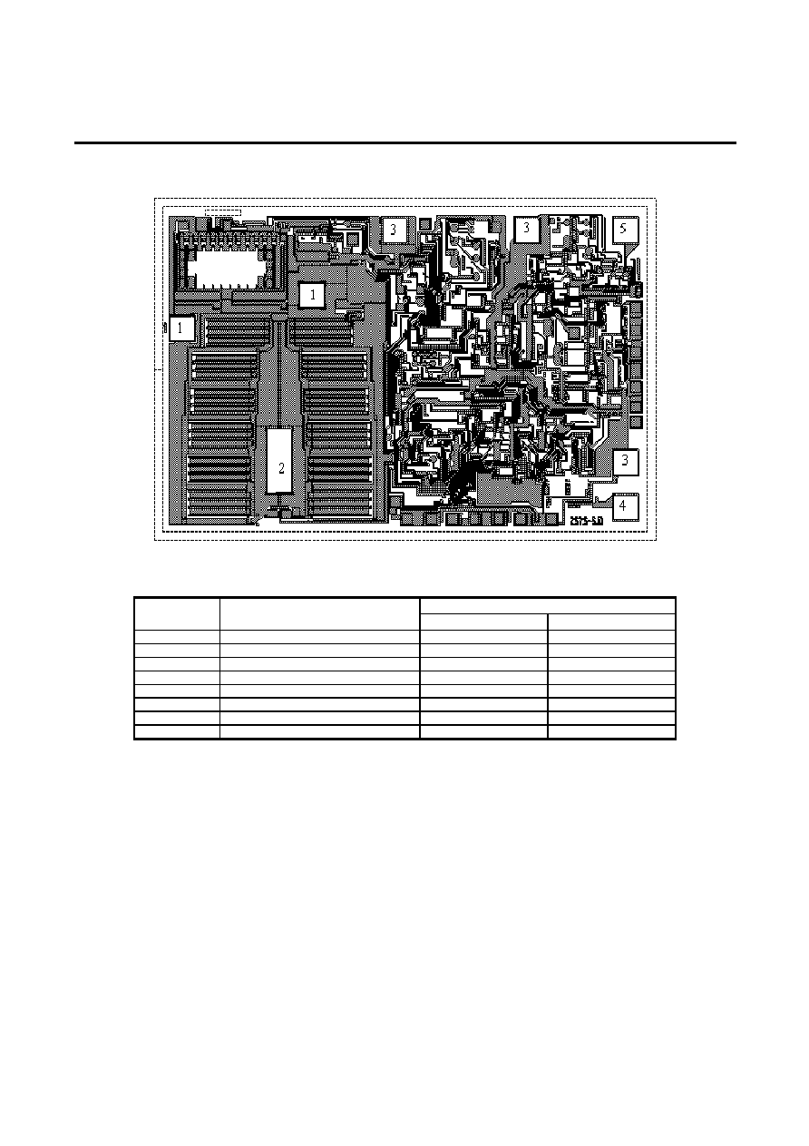
Pad location MIK2575
Chip Size 3.95x2.65mm
Pad Location Coordinates
(the center of pads)
Coordinates (µm)
N
Pad size (µm)
X
Y
1 190x190 220.5
1640
1 190x190 1244
1900
2 190x500 985.5
619.5
3 190x190 1893.5
2399
3 190x190 2935
2403
3 190x190 3716.5
603.5
4 190x190 3716.5
254
5 190x190 3716.5
2399
Page 5 of 5