 | ÐлекÑÑоннÑй компоненÑ: LP3992 | СкаÑаÑÑ:  PDF PDF  ZIP ZIP |
Äîêóìåíòàöèÿ è îïèñàíèÿ www.docs.chipfind.ru
LP3992
Micropower 1.5V CMOS Voltage Regulator with
Shutdown Control
General Description
The LP3992 regulator is designed to meet the requirements
of portable, battery-powered systems providing an accurate
output voltage, low noise, and low quiescent current. Battery
life will be prolonged by the ability of the LP3992 to provide
a 1.5V output from the low input voltage of 1.9V. Additionally,
when switched to a shutdown mode via a logic signal at the
shutdown pin, the power consumption is reduced to virtually
zero. The LP3992 also features short-circuit and thermal-
shutdown protection.
The LP3992 is designed to be stable with space saving
ceramic capacitors as small as 1.0µF.
The device is available in an SOT23-5 package. Perfor-
mance is specified for a -40°C to 125°C temperature range.
For output voltages other than 1.5V and alternative package
options, please contact your local NSC sales office.
Key Specifications
n
1.9 to 5.2V input range
n
Accurate 1.5V
±
0.09V output voltage
n
Less than 1.5µA quiescent current in shutdown
n
Stable with a 1µF output capacitor
n
Guaranteed 30mA output current
n
Low output voltage Noise; 300µV
RMS
Features
n
Operation from a low input voltage; 1.9V
n
Low quiescent current; 29µA typical
n
Stable with a ceramic capacitor
n
Logic controlled shutdown
n
Fast turn ON and OFF
n
Thermal-overload and short circuit protection
n
5 pin package, SOT23
n
-40°C to +125°C junction temperature range
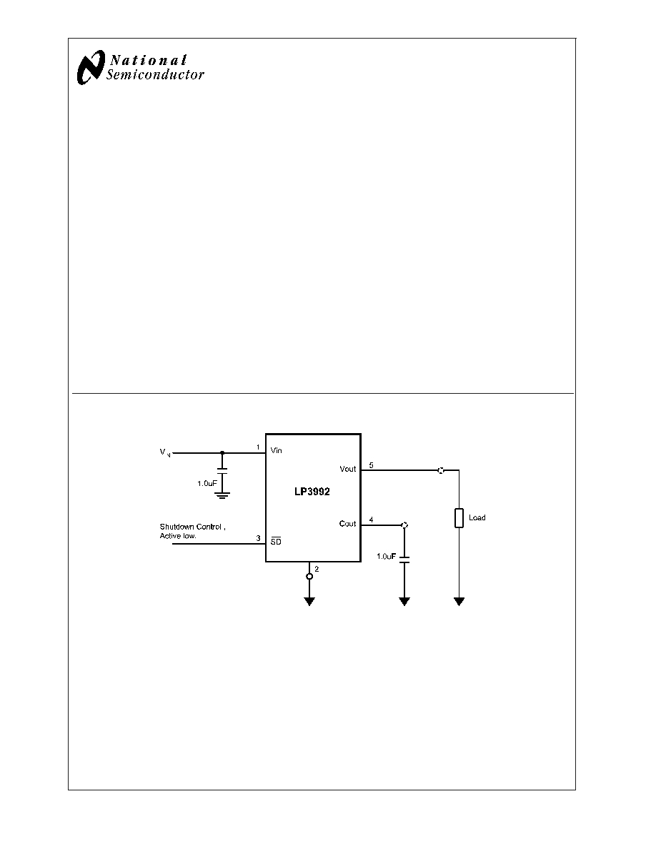
Typical Application Circuit
20041201
December 2002
LP3992
Micropower
1.5V
CMOS
V
oltage
Regulator
with
Shutdown
Control
© 2002 National Semiconductor Corporation
DS200412
www.national.com
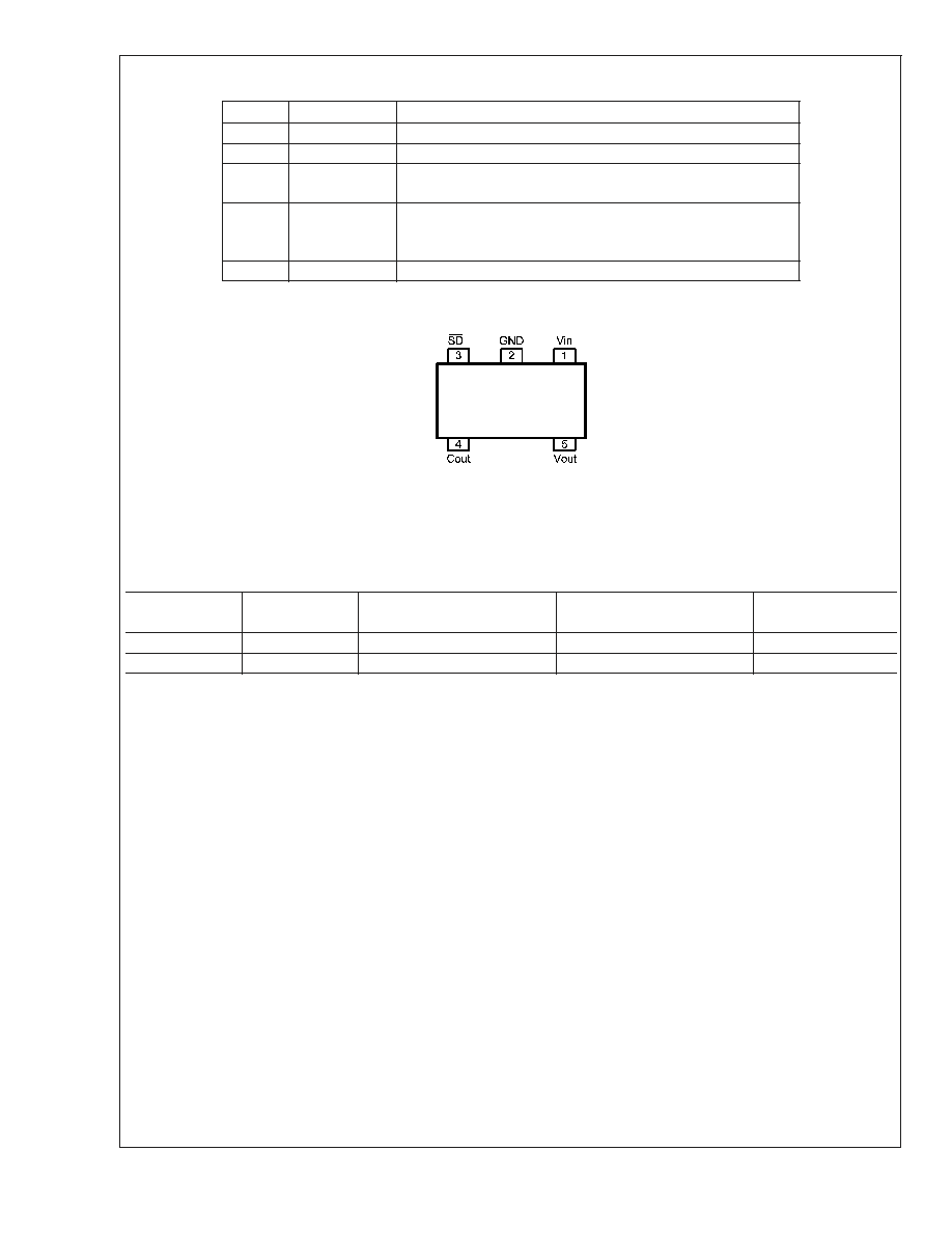
Pin Descriptions
Pin No
Symbol
Name and Function
1
V
IN
Voltage Supply Input
2
GND
Common Ground
3
SD
Shutdown input; Disables the regulator when
0.4V.
Enables the regulator when
1.15V.
4
C
OUT
Output capacitor connection. Internally Connected to V
OUT
connection. This is the recommended device connection for the
1.0µF output capacitor to guarantee a stable output.
5
V
OUT
Voltage output. Connect this output to the load circuit.
Connection Diagram
20041202
SOT23 - 5 Package (MF)
Top View
See NS package number MF05A
Ordering Information
Output
Voltage (V)
Grade
LP3992 Supplied as 1000
Units, Tape and Reel
LP3992 Supplied as 3000
Units, Tape and Reel
Package Marking
1.5
STD
LP3992IMF-1.5
LP3992IMFX-1.5
1.5
STD
LP3992IMF-1.5/E4000193
LP3992IMFX-1.5/S4000170
LP3992
www.national.com
2
Absolute Maximum Ratings
(Notes 1, 2)
If Military/Aerospace specified devices are required,
please contact the National Semiconductor Sales Office/
Distributors for availability and specifications.
Input Voltage
-0.3 to 6.5V
Output Voltage
-0.3 to (V
IN
+ 0.3V) to
6.5V (max)
Shutdown Input Voltage
-0.3 to 6.5V
Junction Temperature
150°C
Lead Temp. (Note 3)
260°C
Storage Temperature
-65 to 150°C
Thermal Resistance (Note 4)
JA
220°C/W
Maximum Power Dissipation
at 25°C
568mW
ESD (Note 5)
Human Body Model
2KV
Machine Model
200V
Operating Conditions
(Note 1)
Input Voltage
1.9 to 5.2V
Shutdown Input Voltage
0 to 6.0V
Junction Temperature
-40°C to 125°C
Power Dissipation at 25°C
454mW
Electrical Characteristics
Unless otherwise noted, V
SD
= 1.15, V
IN
= V
OUT
+ 1.0V, C
IN
= 1 µF, I
OUT
= 1 mA, C
OUT
= 1 µF. Typical values and limits ap-
pearing in normal type apply for T
J
= 25°C. Limits appearing in boldface type apply over the full temperature range for opera-
tion, -40 to +125°C. (Note 13)
Symbol
Parameter
Conditions
Typ
Limit
Units
Min
Max
V
IN
Input Voltage
1.9
5.2
V
V
OUT
Output Voltage Tolerance
Over full line and load regulation.
-90
+90
mV
Line Regulation Error
V
IN
= (V
OUT(NOM)
+ 1.0V) to 5.2V,
I
OUT
= 1mA
-0.27
+0.27
%/V
Load Regulation Error
I
OUT
= 1mA to 30mA
100
220
µV/mA
I
LOAD
Load Current
(Notes 6, 7)
0
µA
I
Q
Quiescent Current
V
SD
= 1.15V, I
OUT
= 0mA
26
50
µA
V
SD
= 1.15V, I
OUT
= 30mA
29
50
V
SD
= 0.4V
0.003
1.5
I
SC
Short Circuit Current Limit
(Note 12)
90
mA
PSRR
Power Supply Rejection Ratio
f = 1kHz, I
OUT
= 30mA
40
dB
f = 20kHz, I
OUT
= 30mA
30
E
EN
Output noise Voltage (Note 7)
BW = 10Hz to 1000kHz,
V
IN
= 4.2V
300
µV
RMS
T
SHUTDOWN
Thermal Shutdown Temperature
160
°C
Thermal Shutdown Hysteresis
20
Enable Control Characteristics
I
SD
Maximum Input Current at
SD Input
V
EN
= 0.0V and V
IN
= 5.2V
0.001
µA
V
IL
Low Input Threshold
V
IN
= 1.8V to 5.2V
0.4
V
V
IH
High Input Threshold
V
IN
= 1.8 to 5.2V
1.15
V
Timing Characteristics
T
ON1
Turn On Time (Note 7)
50 to 85% of V
OUT(NOM)
(Note 8)
15
µS
T
ON2
To 95% Level (Note 9)
40
T
OFF1
Turn Off Time (Note 7)
85 to 50% of V
OUT(NOM)
(Note 10)
15
µS
T
OFF2
95 to 5% Level (Note 11)
40
Transient
Response
Line Transient Response |
V
OUT
| T
rise
= T
fall
= 10µS (Note 7)
60
mV
Load Transient Response
|
V
OUT
|
T
rise
= T
fall
= 1µS
I
OUT
= 100µA to 5mA(Note 7)
60
Note 1: Absolute Maximum Ratings are limits beyond which damage can occur. Operating Ratings are conditions under which operation of the device is
guaranteed. Operating Ratings do not imply guaranteed performance limits. For guaranteed performance limits and associated test conditions, see the Electrical
Characteristics tables.
Note 2: All Voltages are with respect to the potential at the GND pin.
LP3992
www.national.com
3
Electrical Characteristics
(Continued)
Note 3: The package can pass MSL (moisture sensitivity level) 1 at 260°C.
Additional information on lead temperature can be obtained from National Semiconductor web pages
http://www.national.com/packaging/general.html
http://www.national.com/packaging/plastic.html
Note 4: The Maximum power dissipation of the device is dependant on the maximum allowable junction temperature for the device and the ambient temperature.
This relationship is given by the formula
P
D
= (T
J
- T
A
)/
JA
Where T
J
is the junction temperature, T
A
is the ambient temperature, and
JA is the junction-to-ambient thermal resistance. The Maximum Power dissipation across
the device related to the operational conditions can be calculated using the formula
P
D
= (V
IN(MAX)
- V
OUT(MAX)
) * (I
OUT(MAX)
)
Substituting the device values gives the max power dissipation = (5.2V - 1.5V)(0.03) = 0.111W. This figure for Maximum power dissipation can be used to derive the
maximum ambient temperature. For the SOT23-5 package
JA
= 220°C/W, thus for this device the maximum temperature difference, (T
J
- T
A
), is 24.4°C, (0.111 *
220). This gives the maximum ambient temperature for operation as 100.6°C, (125 - 24.4). Similarly the numbers for the absolute maximum case can be derived
using a figure of 150°C for the junction temperature.
Note 5: The human body is 100pF discharge through 1.5kW resistor into each pin. The machine model is a 200 pF capacitor discharged directly into each pin.
Note 6: The device maintains the regulated output voltage without the load.
Note 7: This electrical specification is guaranteed by design.
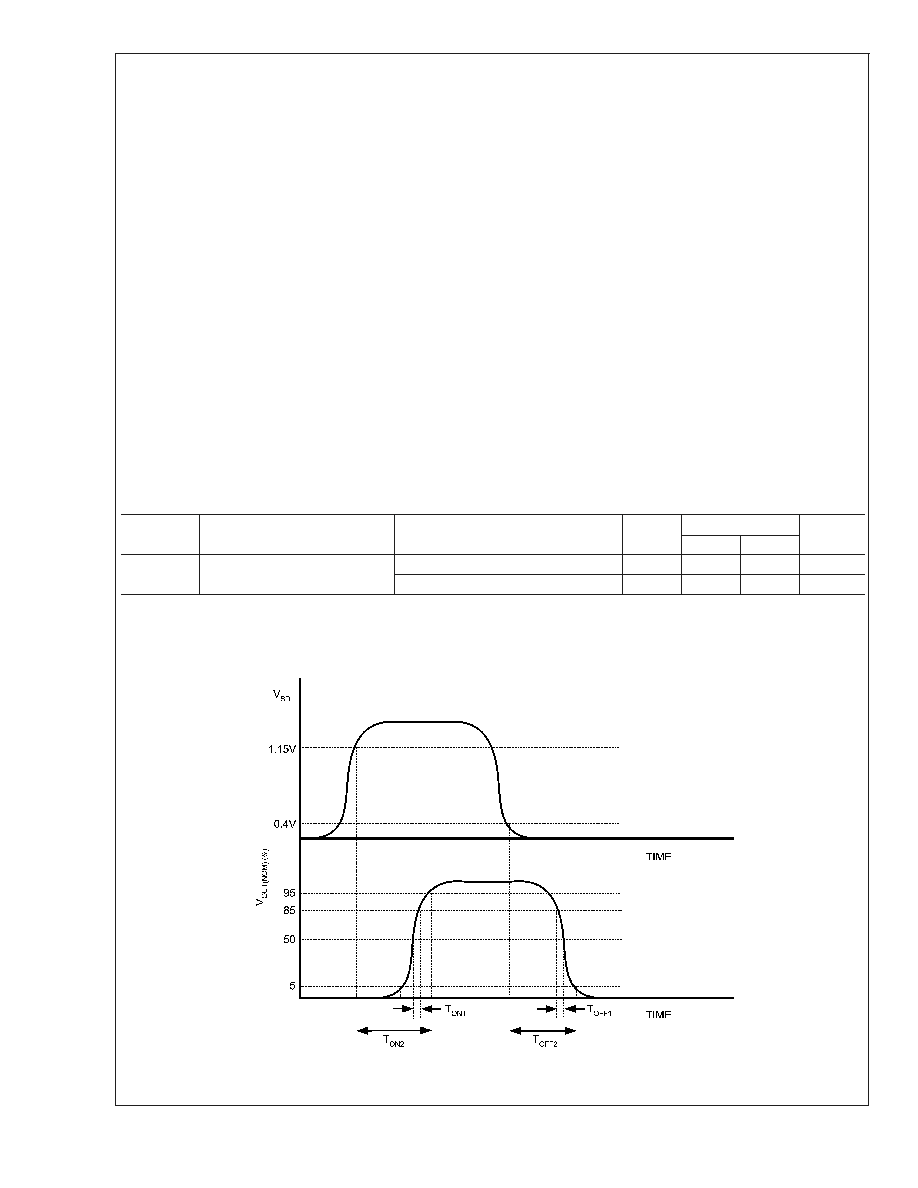
Note 8: Time for V
OUT
to rise from 50 to 85% of V
OUT(nom)
. (figure 1)
Note 9: Time from V
SD
= 1.15V to V
OUT
= 95%(V
OUT(nom)
). (figure 1)
Note 10: Time for V
OUT
to fall from 85 to 50% of V
OUT(nom)
. (figure 1)
Note 11: Time from V
SD
= 0.4V to V
OUT
= 5%(V
OUT(nom)
. (figure 1)
Note 12: Short circuit current is measured on the input supply line at the point when the short circuit condition reduces the output voltage to 95% of its nominal value.
Note 13: All limits are guaranteed. All electrical characteristics having room-temperature limits are tested during production at T
J
= 25°C or correlated using
Statistical Quality Control methods. Operation over the temperature specification is guaranteed by correlating the electrical characteristics to process and
temperature variations and applying statistical process control.
Output Capacitor, Recommended Specifications
Symbol
Parameter
Conditions
Typ
Limit
Units
Min
Max
C
o
Output Capacitor
Capacitance(Note 14)
1.0
µF
ESR
5
500
m
Note 14: Capacitor types recommended are X7R, Y5V, and Z5U. X7R tolerance is quoted as 15% over temperature.
20041203
FIGURE 1. Figure 1. T
on
/T
off
Timing Diagram
LP3992
www.national.com
4
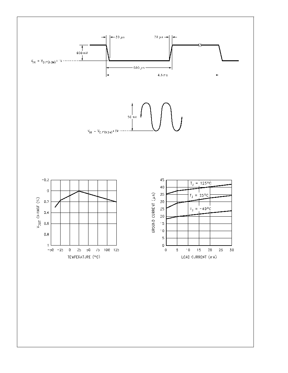
Typical Performance Characteristics.
Unless otherwise specified, C
IN
= C
OUT
= 1.0 µF Ceramic,
V
IN
= 2.8V, T
A
= 25°C, Shutdown pin is tied to V
IN
.
Output Voltage Change vs Temperature
Ground Current vs Load Current
20041207
20041208
20041204
FIGURE 2. Figure 2. Line Transient Input Test Signal.
20041205
FIGURE 3. Figure 3. PSRR Input Test Signal.
LP3992
www.national.com
5
Document Outline