 | –≠–ª–µ–∫—Ç—Ä–æ–Ω–Ω—ã–π –∫–æ–º–ø–æ–Ω–µ–Ω—Ç: LM2935 | –°–∫–∞—á–∞—Ç—å:  PDF PDF  ZIP ZIP |
Low Dropout
Dual Voltage Regulator
The LM2935 is a dual positive 5.0 V low dropout voltage regulator,
designed for standby power systems. The main output is capable of
supplying 750 mA for microprocessor power, and can be turned "on"
and "off" by the switch/reset input. The other output is dedicated for
standby operation of volatile memory, and is capable of supplying up
to 10 mA loads. The total device features a low quiescent current of
3.0 mA or less when supplying 10 mA from the standby output.
This part was designed for harsh automotive environments and is
therefore immune to many input supply voltage problems such as
reverse battery (≠12 V), double battery (+24 V), and load dump
transients (+60 V).
∑
Two Regulated 5.0 V Outputs
∑
Main Output Current in Excess of 750 mA
∑
On/Off Control of Main Output
∑
Standby Output Current in Excess of 10 mA
∑
Low Input/Output Differential of Less than 0.6 V at 500 mA
∑
Short Circuit Current Limiting
∑
Internal Thermal Shutdown
∑
Low Voltage Indicator Output
∑
Designed for Automotive Environment Including
∑
Reverse Battery Protection
∑
Double Battery Protection
∑
Load Dump Protection
∑
Reverse Transient Protection
∑
Economical 5≠Lead TO≠220 Package with Two Optional Leadforms
∑
Also Available in Surface Mount D
2
PAK Package
ORDERING INFORMATION
Device
Operating
Temperature Range
Package
LM2935D2T
Surface Mount
LM2935T
T = 40
∞
to +125
∞
C
Plastic Power
LM2935TH
T
J
= ≠40
∞
to +125
∞
C
Horizontal Mount
LM2935TV
Vertical Mount
ON Semiconductort
©
Semiconductor Components Industries, LLC, 2001
April, 2001 ≠ Rev. 2
1
Publication Order Number:
LM2935/D
LM2935
SEMICONDUCTOR
TECHNICAL DATA
LOW DROPOUT
DUAL VOLTAGE REGULATOR
1
5
TV SUFFIX
PLASTIC PACKAGE
CASE 314B
T SUFFIX
PLASTIC PACKAGE
CASE 314D
TH SUFFIX
PLASTIC PACKAGE
CASE 314A
Heatsink surface connected to Pin 3.
5
1
D2T SUFFIX
PLASTIC PACKAGE
CASE 936A
(D
2
PAK)
Pin 1. Input Voltage/V
CC
2. Main Output
3. Ground
4. Switch/Reset
5. Standby/Output
Heatsink surface (shown as terminal 6
in case outline drawing) is connected to Pin 3.
5
1
5
1
LM2935
http://onsemi.com
2
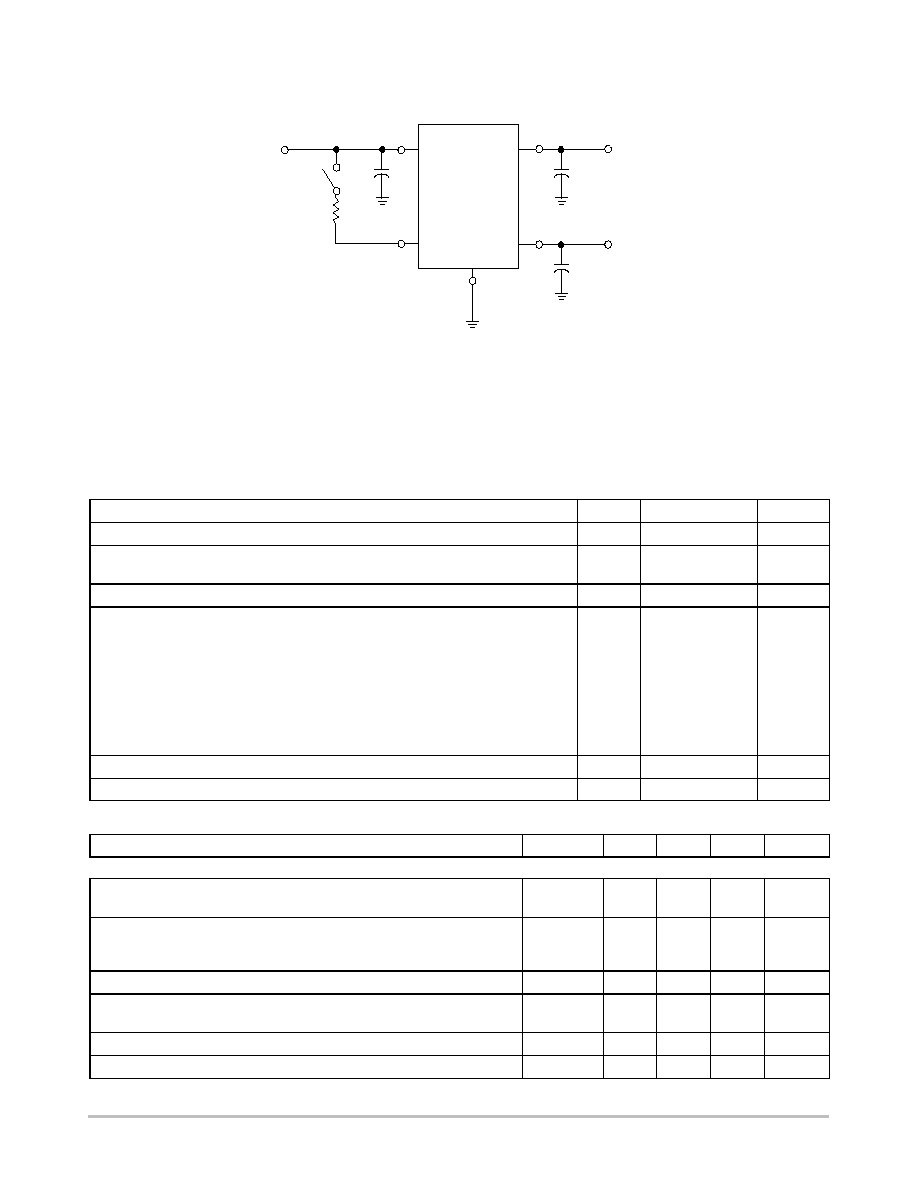
*The main output
is Off" with switch
S1 open.
An input bypass capacitor is recommended if the regulator is located more than 4
from the supply
input filter. The LM2935 is not internally compensated and thus requires an external output capacitor
for stability. A minimum capacitance of 10
µ
F is recommended. The actual capacitance value is
dependent upon load current, temperature, and the capacitor's equivalent series resistance (ESR).
The least stable condition is encountered at maximum load current and minimum ambient
temperature.
V
in
S1*
0.1
Input
Switch/
Reset
Gnd
3
1
4
Standby
Main
Output
2
20 k
LM2935
5.0 V/750 mA
+
10
Typical Application Circuit
This device contains 29 active transistors.
5
5.0 V/10 mA
+
10
MAXIMUM RATINGS
Rating
Symbol
Value
Unit
Input Voltage Continuous
V
I
60
Vdc
Transient Reverse Polarity Input Voltage
1.0% Duty Cycle,
100 ms
≠V
I
(
)
≠50
Vpk
Switch/Reset Input Current
I
in
5.0
mA
Power Dissipation
Case 314A, 314B and 314D (TO≠220 Type)
T
A
= 25
∞
C
P
D
Internally Limited
W
Thermal Resistance, Junction≠to≠Ambient
R
JA
65
∞
C/W
Thermal Resistance, Junction≠to≠Case
R
JC
5.0
∞
C/W
Case 936A (D
2
PAK)
T
A
= 25
∞
C
P
D
Internally Limited
W
Thermal Resistance, Junction≠to≠Ambient
R
JA
Per Figure 1
∞
C/W
Thermal Resistance, Junction≠to≠Case
R
JC
5.0
∞
C/W
Operating Junction Temperature Range
T
J
≠40 to +150
∞
C
Storage Temperature Range
T
stg
≠65 to +150
∞
C
ELECTRICAL CHARACTERISTICS
(V
in
= 14 V, I
O
= 500 mA, I
stby
= 0 mA, C
O
= 10
µ
F, C
stby
= 10
µ
F, T
J
= 25
∞
C [Note 1].)
Characteristic
Symbol
Min
Typ
Max
Unit
MAIN OUTPUT
Output Voltage (V
in
= 6.0 V to 26 V, I
O
= 5.0 mA to 500 mA, T
J
= ≠40 to
+125
∞
C)
V
O
4.75
5.0
5.25
V
Line Regulation
V
in
= 9.0 V to 16 V, I
O
= 5.0 mA
V
in
= 6.0 V to 26 V, I
O
= 5.0 mA
Reg
line
≠
≠
4.0
10
25
50
mV
Load Regulation (I
O
= 5.0 mA to 500 mA)
Reg
load
≠
10
50
mV
Output Impedance
I
O
= 500 mAdc and 10 mArms, f = 100 Hz to 10 kHz
Z
O
≠
200
≠
m
Output Noise Voltage (f = 10 Hz to 100 kHz)
V
n
≠
100
≠
µ
Vrms
Long Term Stability
S
≠
20
≠
mV/kHR
LM2935
http://onsemi.com
3
ELECTRICAL CHARACTERISTICS
(V
in
= 14 V, I
O
= 500 mA, I
stby
= 0 mA, C
O
= 10
µ
F, C
stby
= 10
µ
F, T
J
= 25
∞
C [Note 1].)
Characteristic
Unit
Max
Typ
Min
Symbol
MAIN OUTPUT (continued)
Ripple Rejection (f = 120 Hz)
RR
≠
66
≠
dB
Dropout Voltage
I
O
= 500 mA
I
O
= 750 mA
V
I
≠V
O
≠
≠
0.45
0.82
0.6
≠
V
Short Circuit Current Limit
I
SC
0.75
1.2
≠
A
Over≠Voltage Shutdown Threshold
V
th(OV)
26
31
≠
V
SWITCH/RESET
Output Sink Current (V
OL
= 1.2 V)
I
Sink
≠
5.0
≠
mA
Output Voltage (R
on/off
= 20 k
)
Low State, V
in
= 4.0 V
High State, V
in
= 14 V
V
OL
V
OH
≠
4.5
0.9
5.0
1.2
6.0
V
Output Pull≠Up Resistor, "On"/"Off" (Note 2)
R
on/off
≠
20
30
k
Output Voltage with Reverse Polarity Input (V
in
= ≠15 V, R
L
=
10
)
≠V
O
≠0.6
0
≠
V
ELECTRICAL CHARACTERISTICS
(V
in
= 14 V, I
O
= 0 mA, I
stby
= 10 mA, C
O
= 10
µ
F, C
stby
= 10
µ
F, T
J
= 25
∞
C [Note 1].)
Characteristic
Symbol
Min
Typ
Max
Unit
STANDBY OUTPUT
Output Voltage (V
in
= 6.0 V to 26 V, I
stby
= 1.0 mA to 10 mA, T
J
= ≠40 to
+125
∞
C)
V
O(stby)
4.75
5.0
5.25
V
Tracking Voltage
V
O
≠V
O(stby)
≠200
0
200
mV
Line Regulation (V
in
= 6.0 V to 26 V)
Reg
line
≠
4.0
50
mV
Load Regulation (I
stby
= 1.0 mA to 10 mA)
Reg
load
≠
10
50
mV
Output Impedance
I
(stby)
= 10 mAdc and 1.0 mArms, f = 100 Hz to 10 kHz
Z
O(stby)
≠
1.0
≠
Output Noise Voltage (f = 10 Hz to 100 kHz)
V
n
≠
300
≠
µ
Vrms
Long Term Stability
S
≠
20
≠
mV/kHR
Ripple Rejection (f = 120 Hz)
RR
≠
66
≠
dB
Dropout Voltage (I
stby
= 10 mA)
V
I
≠V
O(stby)
≠
0.55
0.7
V
Short Circuit Current Limit
I
SC
25
70
≠
mA
Output Voltage with Reverse Polarity Input
V
in
= ≠15 V, R
L
=
510
≠V
O
≠0.3
0
≠
V
Output Voltage with Maximum Positive Input
V
in
= 60 V, R
L
= 510
V
O(max)
≠
5.0
6.0
V
TOTAL DEVICE
Bias Current
I
O
= 10 mA, I
stby
= 0 mA
I
O
= 500 mA, I
stby
= 0 mA
I
O
= 750 mA, I
stby
= 0 mA
Main Output "Off", I
stby
= 10 mA
I
B
≠
≠
≠
≠
3.0
40
90
2.0
≠
100
≠
3.0
mA
NOTES: 1. Low duty cycle pulse techniques are used during test to maintain junction temperature as close to ambient as possible.
2. The maximum switch/reset current must not exceed 5.0 mA.
LM2935
http://onsemi.com
4
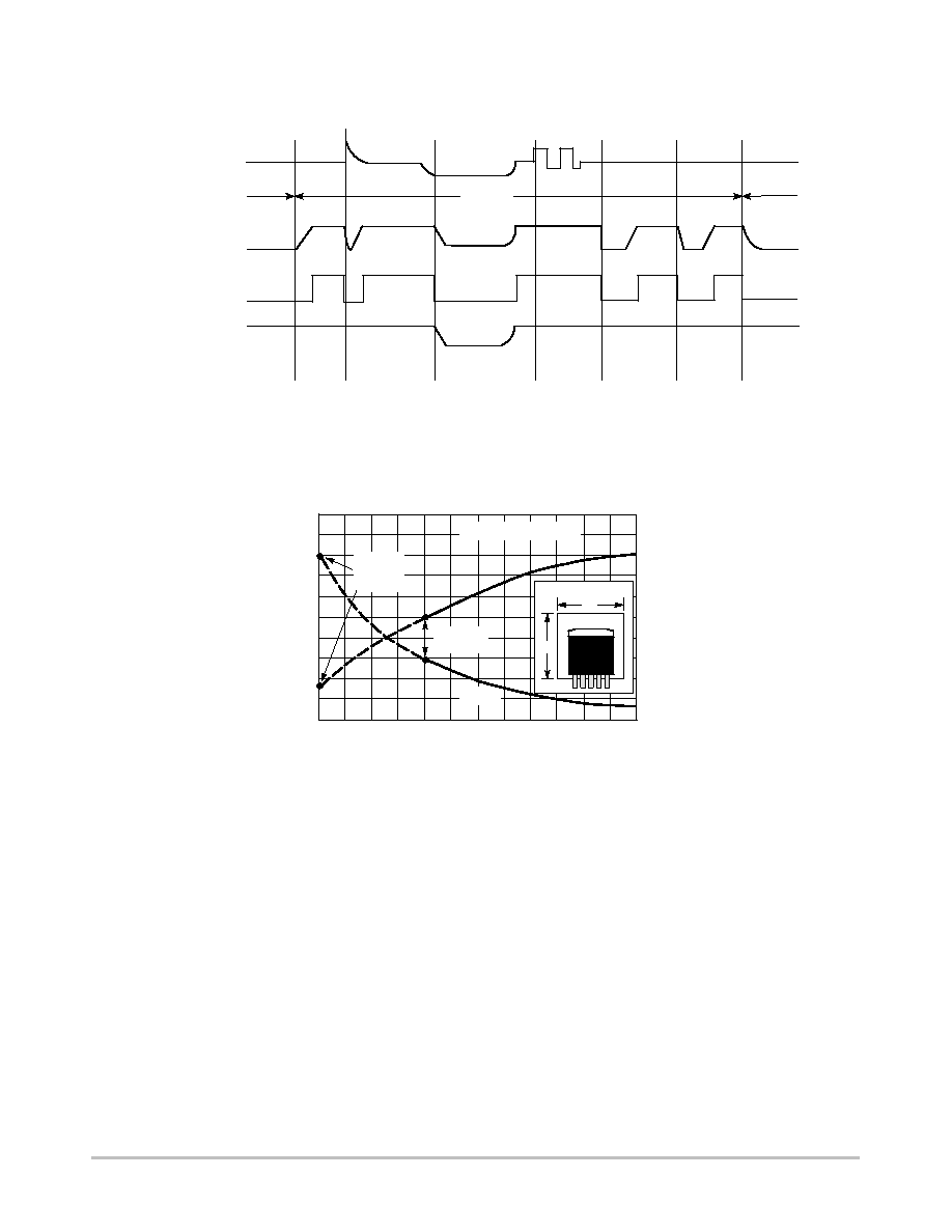
V
in
, Input Voltage
(Pin 1)
S1, On"/Off" Switch
V
O
, Main Output Voltage
(Pin 2)
Reset (Pin 4)
V
stby
, Standby Voltage
(Pin 5)
Open
Main
Output
Turn On"
Load
Dump
Low Input
Voltage
Input
Voltage
Line Noise
Main
Output
Short
Circuit
Thermal
Shutdown
Main
Output
Turn Off"
Open
Closed
60 V
14 V
3.0 V
5.0 V
2.4 V
0 V
9.0 V
14 V
14 V
5.0 V
5.0 V
5.0 V
5.0 V
5.0 V
5.0 V
5.0 V
0 V
2.4 V
26 V
TYPICAL CIRCUIT WAVEFORMS
R
,
THERMAL
RESIST
ANCE
JA
JUNCTION-T
O-AIR ( C/W)
∞
30
40
50
60
70
80
1.0
1.5
2.0
2.5
3.0
3.5
0
10
20
30
25
15
5.0
L, LENGTH OF COPPER (mm)
P
D(max)
for T
A
= 50
∞
C
Minimum
Size Pad
2.0 oz. Copper
L
L
ŒŒŒŒ
ŒŒŒŒ
ŒŒŒŒ
ŒŒŒŒ
Free Air
Mounted
Vertically
P D
, MAXIMUM POWER DISSIP
A
TION (W)
R
JA
Figure 1. D
2
PAK Thermal Resistance and Maximum
Power Dissipation versus P.C.B. Copper Length
LM2935
http://onsemi.com
5
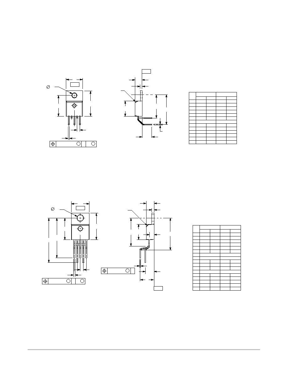
PACKAGE DIMENSIONS
TH SUFFIX
PLASTIC PACKAGE
CASE 314A≠03
ISSUE E
NOTES:
1. DIMENSIONING AND TOLERANCING PER ANSI
Y14.5M, 1982.
2. CONTROLLING DIMENSION: INCH.
3. DIMENSION D DOES NOT INCLUDE
INTERCONNECT BAR (DAMBAR) PROTRUSION.
DIMENSION D INCLUDING PROTRUSION SHALL
NOT EXCEED 0.043 (1.092) MAXIMUM.
DIM
A
MIN
MAX
MIN
MAX
MILLIMETERS
0.572
0.613 14.529 15.570
INCHES
B
0.390
0.415
9.906 10.541
C
0.170
0.180
4.318
4.572
D
0.025
0.038
0.635
0.965
E
0.048
0.055
1.219
1.397
F
0.570
0.585 14.478 14.859
G
0.067 BSC
1.702 BSC
J
0.015
0.025
0.381
0.635
K
0.730
0.745 18.542 18.923
L
0.320
0.365
8.128
9.271
Q
0.140
0.153
3.556
3.886
S
0.210
0.260
5.334
6.604
U
0.468
0.505 11.888 12.827
≠T≠
SEATING
PLANE
L
S
E
C
F
K
J
OPTIONAL
CHAMFER
5X
D
5X
M
P
M
0.014 (0.356)
T
G
A
U
B
Q
≠P≠
TV SUFFIX
PLASTIC PACKAGE
CASE 314B≠05
ISSUE J
V
Q
K
F
U
A
B
G
≠P≠
M
0.10 (0.254)
P
M
T
5X
J
M
0.24 (0.610)
T
OPTIONAL
CHAMFER
S
L
W
E
C
H
N
≠T≠
SEATING
PLANE
NOTES:
1. DIMENSIONING AND TOLERANCING PER ANSI
Y14.5M, 1982.
2. CONTROLLING DIMENSION: INCH.
3. DIMENSION D DOES NOT INCLUDE
INTERCONNECT BAR (DAMBAR) PROTRUSION.
DIMENSION D INCLUDING PROTRUSION SHALL
NOT EXCEED 0.043 (1.092) MAXIMUM.
DIM
MIN
MAX
MIN
MAX
MILLIMETERS
INCHES
A
0.572
0.613 14.529 15.570
B
0.390
0.415
9.906 10.541
C
0.170
0.180
4.318
4.572
D
0.025
0.038
0.635
0.965
E
0.048
0.055
1.219
1.397
F
0.850
0.935 21.590 23.749
G
0.067 BSC
1.702 BSC
H
0.166 BSC
4.216 BSC
J
0.015
0.025
0.381
0.635
K
0.900
1.100 22.860 27.940
L
0.320
0.365
8.128
9.271
N
0.320 BSC
8.128 BSC
Q
0.140
0.153
3.556
3.886
S
---
0.620
--- 15.748
U
0.468
0.505 11.888 12.827
V
---
0.735
--- 18.669
W
0.090
0.110
2.286
2.794
5X
D