
Voice Controllerr 1 / 1 Issue Date : 27 March,2000
Syntek Semiconductor Co., Ltd.
STK88C2441
Specification
1. FEATURES
* Operating voltage : 2.5V - 5.5V.
* Maximum CPU operating frequency : 4,194,304Hz at 2.7V.
* Provide X'tal or RC oscillator. Both can run at high speed or slow speed(low power).
RC oscillator can detect internal or external resister automatically.
* Support 4M bytes program and data ROM. 256K bytes of them are built-in.
* Built in 128 bytes RAM.
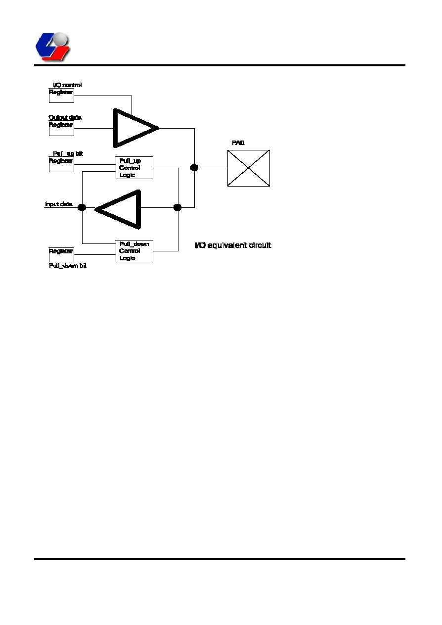
* I/O port.
-
24 I/O pins.
-
8 of 24 pins with wake up function.
* Six 8-bit timers.
* Four channels for voice or melody processing.
* Two DACs for voice or melody playing. Also, internal programming for single DAC
playing.
* One pair of PWM for voice or melody playing.
* Eight interrupt sources :
NMI - Can be Watchdog Timer interrupt
IRQ0 - Timer 0 interrupt
IRQ1 - Timer 1 interrupt
IRQ2 - Timer 2 interrupt
IRQ3 - Timer 3 interrupt
IRQ4 - Timer 4 interrupt
IRQ5 - External interrupt
IRQ6 -
Base Timer interrupt
IRQ7 -
Timer 5 interrupt

Voice Controllerr 2 / 2 Issue Date : 27 March,2000
Syntek Semiconductor Co., Ltd.
STK88C2441
2. PIN NAME ASSIGNMENT ( Total: 62 pads )
Pin Name
I/O
Function description
1)
PA0~PA7
I/O
8-bit I/O pins for port 1 with wake-up interrupt
2)
PB0~PB7
I/O
8-bit I/O pins for port 2.
3)
PC0~PC7
I/O
8-bit I/O pins for port 3. PC0-PC7 will changed to BANK0-
BANK7 output if bank number is less than $F0 or /DIROM=0.
4)
A0-A13
O
Address bus.
5)
D0-D7
I/O
Data bus.
6)
CEB
O
External ROM chip enable.
7)
/EXTROM
I
=0 Disable internal ROM.
=1 Enable internal ROM if bank number is greater than $EF.
8)
DAC1
O
Current output port
9)
DAC2
O
Current output port
10)
PWM1
O
Voltage output port
11)
PWM2
O
Voltage output port
12)
VCOCAP
I/O
PLL used.
13)
RXOSC
I
X'TAL or Ring osc pad
14)
XOSC2
O
X'TAL pad
15)
XR
I
Bias input for RC oscillator.
16)
RESB
I
System reset pin; internal pull_high.
17)
TESTB
I
Test pin; internal pull_high.
18)
VDD
I
Power
19)
VDD(PWM)
I
Power for PWM module
20)
GND
I
Ground
21)
GND(PWM)
I
Ground for PWM module
3. ADDRESS ARRANGEMENT
1) RAM
0000-007F for data storage.
0100-017F for stack and data area.. This area is overlapped with 0000-007F.
2) ROM
Max. 4M bytes for program and speech data area.
This area splits into 256 banks (0~255). There are 16k bytes for every bank. The
last 16 banks (240-255) are built-in. If /DIROM=1 and bank number is greater
than $EF, then internal ROM is read. If /DIROM=0 or bank number is less than

Voice Controllerr 3 / 3 Issue Date : 27 March,2000
Syntek Semiconductor Co., Ltd.
STK88C2441
$F0, then external ROM is read.
Internal ROM related address shows below:
BANK numberCPU address Internal ROM address
bank 240
11110000
8000-BFFF
00000-03FFF
bank 241
11110001
8000-BFFF
04000-07FFF
bank 242
11110010
8000-BFFF
08000-0BFFF
...............................................................................
bank 255
11111111
8000-BFFF
3C000-3FFFF
(bank 255
11111111
C000-FFFF
3C000-3FFFF)
If RESET or IRQ or NMI or Bank address=FF, ROM address will indicate to 3C000-3FFFF.
FFFF, FFFE - IRQ vector.
FFFD, FFFC - RES vector.
FFFB, FFFA - NMI vector for watchdog interrupt.
4. Register description
(1) Read and Write
00C0
IRQ flag register. Read & write.
Read function :
Bit 0 :
= 1 Timer 0 flag, IRQ 0.
1 :
= 1 Timer 1 flag, IRQ 1
2 :
= 1 Timer 2 flag, IRQ 2.
3 :
= 1 Timer 3 flag, IRQ 3.
4 :
= 1 Timer 4 flag, IRQ 4.
5 :
= 1 External flag, IRQ5.
6 :
= 1 Base Timer flag, IRQ6
7 :
= 1 Timer 5 flag, IRQ7.
Write function :
Bit 0 :
= 0 Clear timer 0 flag.
1 :
= 0 Clear timer 1 flag.
2 :
= 0 Clear timer 2 flag.
3 :
= 0 Clear timer 3 flag.
4 :
= 0 Clear timer 4 flag.
5 :
= 0 Clear External flag.
6 :
= 0 Clear Base Timer flag.
7 :
= 0 Clear timer 5 flag..

Voice Controllerr 4 / 4 Issue Date : 27 March,2000
Syntek Semiconductor Co., Ltd.
STK88C2441
00C1
Port A data. Read & write.
00C2
Port A external interrupt high to low transient indicating flag. Read & write.
(Falling edge)
Read function:
Bit 0 : 1 Indicate PA0 transient from high to low FLAG.
Bit 1 : 1 Indicate PA1 transient from high to low FLAG.
Bit 2 : 1 Indicate PA2 transient from high to low FLAG.
Bit 3 : 1 Indicate PA3 transient from high to low FLAG.
Bit 4 : 1 Indicate PA4 transient from high to low FLAG.
Bit 5 : 1 Indicate PA5 transient from high to low FLAG.
Bit 6 : 1 Indicate PA6 transient from high to low FLAG.
Bit 7 : 1 Indicate PA7 transient from high to low FLAG.
* These flags will be cleared by clear external interrupt flag.
Write function:
Bit 0 : 0 Disable and clear PA0 transient high to low flag
Bit 1 : 0 Disable and clear PA1 transient high to low flag
Bit 2 : 0 Disable and clear PA2 transient high to low flag
Bit 3 : 0 Disable and clear PA3 transient high to low flag
Bit 4 : 0 Disable and clear PA4 transient high to low flag
Bit 5 : 0 Disable and clear PA5 transient high to low flag
Bit 6 : 0 Disable and clear PA6 transient high to low flag
Bit 7 : 0 Disable and clear PA7 transient high to low flag
*
The default value for each bit is 0.
00C3
Port A external interrupt low to high transient indicating flag. Read & write
(Rising edge)
Read function:
Bit 0 : 1 Indicate PA0 transient from low to high flag.
Bit 1 : 1 Indicate PA1 transient from low to high flag.
Bit 2 : 1 Indicate PA2 transient from low to high flag.
Bit 3 : 1 Indicate PA3 transient from low to high flag.
Bit 4 : 1 Indicate PA4 transient from low to high flag.
Bit 5 : 1 Indicate PA5 transient from low to high flag.
Bit 6 : 1 Indicate PA6 transient from low to high flag.
Bit 7 : 1 Indicate PA7 transient from low to high flag.
* These flags will be cleared by clear external interrupt flag.

Voice Controllerr 5 / 5 Issue Date : 27 March,2000
Syntek Semiconductor Co., Ltd.
STK88C2441
Write function:
Bit 0 : 0 Disable and clear PA0 transient low to high flag
Bit 1 : 0 Disable and clear PA1 transient low to high flag
Bit 2 : 0 Disable and clear PA2 transient low to high flag
Bit 3 : 0 Disable and clear PA3 transient low to high flag
Bit 4 : 0 Disable and clear PA4 transient low to high flag
Bit 5 : 0 Disable and clear PA5 transient low to high flag
Bit 6 : 0 Disable and clear PA6 transient low to high flag
Bit 7 : 0 Disable and clear PA7 transient low to high flag
*
The default value for each bit is 0.
00C4
Port B data. Read & write.
00C5
Port C data. Read & write.
00CF
Timer 5 data. Write only.
*
After timer 5 been enabled, the timer will start to count down. When
timer counts to 0, the timer will count from the initial value and IRQ7
will happen.
*
If any bit of ($00D9) is set to 1, then timer 5 IRQ will be disabled.
*
Valid values are from 1 to 255. 0 is prohibited.
*
Timer 5 input clock is system_clock.
*
The time elapse = ($00CF) / system_clock.
*
The timer 5 can be used as carrier generator. The carrier frequency is
(system clock) / ($00CF) / 2
(2) Port definition
00D0
Set port A bit function. Write only.
*
An '1' in this register will set the corresponding pin of port A as an output pin.
*
The default value for each bit is 0.
00D1
Set port A pull-up resistor. Write only.
*
An '1' in this register will enable the pull-up resistor of the corresponding pin of port A. But the
pull-up resistor will be disabled if the pin is output low.
*
The default value for each bit is 0.
00D5
Set port B bit function. Write only.

Voice Controllerr 6 / 6 Issue Date : 27 March,2000
Syntek Semiconductor Co., Ltd.
STK88C2441
*
An '1' in this register will set the corresponding pin of port B as an output pin.
*
The default value for each bit is 0.
00D6
Set port B pull-up resistor. Write only.
*
An '1' in this register will enable the pull-up resistor of the corresponding pin of port B. But the
pull-up resistor will be disabled if the pin is output low.
*
The default value for each bit is 0.
00D9
Port B bitwise output type function selection. Write only.
Bit
[7:0]= 0 set this pin as a buffer type output buffer.
0 : = 1 Carrier frequency is inserted while data=1
1 : = 1 Carrier frequency is inserted while data=0
2 : = 1 Carrier frequency is inserted while data=1
3 : = 1 Carrier frequency is inserted while data=0
4 : = 1 Carrier frequency is inserted while data=1
5 : = 1 Carrier frequency is inserted while data=0
6 : = 1 Carrier frequency is inserted while data=1
7 : = 1 Carrier frequency is inserted while data=0
*
The default value for each bit is 0.
00DA
Set port C bit function. Write only.
*
An '1' in this register will set the corresponding pin of port C as an output pin.
*
The default value for each bit is 0.
00DB
Set port C pull-up resistor. Write only.
*
An '1' in this register will enable the pull-up resistor of the corresponding pin of port C. But the
pull-up resistor will be disabled if the pin is output low.
* The default value for each bit is 0.
00DD
Clear watchdog timer. Write only.
Watchdog timer is about (System_clk/4)/128/256.
00DE
IRQ selection. Write only.
Bit 5:
=0
: Normal IRQ vector
=1
: 7 level IRQ vectors.
6:
=0
: Timer0 INT=IRQ

Voice Controllerr 7 / 7 Issue Date : 27 March,2000
Syntek Semiconductor Co., Ltd.
STK88C2441
=1
: Timer0 INT=NMI
7:
=0
: Base Timer INT=IRQ
=1
: Base Timer INT=NMI
Note : Please note that do not assign two NMI sources at the same time, otherwise the NMI source can
not be identified in software.
00DF
Time base control. Write only.
Bit 0:
=0
: Disable and reset base timer IRQ.
=1
: Enable base timer IRQ
2-1: If Bit[3]=0
=00
: system_clock/1024(resetable)
=01
: system_clock/4096(resetable)
=10
: system_clock/16384(resetable)
=11
: system_clock/65536(resetable)
If Bit[3]=1
=00
: 128Hz( resetable )
=01
: 32Hz( resetable )
=10
: 8Hz( resetable )
=11
: 2Hz( resetable )
3:
=0
: base timer clock = system_clock
=1
: base timer clock=32768Hz
(3)
Control register
00E0
To enter standby mode. Write only.
00E1
To enter sleep mode. Write only.
In sleep mode, the main system oscillator will be stopped. So, all function are stopped and only
external interrupt can wake up this chip.
00E3
Bank select register. Write only.
*
The default bank value is FFH.
00E4
Audio Control register. Write only.
Bit 0 : = 0
Disable DAC1 and DAC2.
= 1
Enable DAC1 and DAC2.
1 : = 0
DAC1 and DAC2 is merged.
= 1
DAC1 and DAC2 is separated.

Voice Controllerr 8 / 8 Issue Date : 27 March,2000
Syntek Semiconductor Co., Ltd.
STK88C2441
2 : = 0
Disable
PWM.
= 1
Enable
PWM
4-3 :If bit[5]=0
= 00
1.70mA(full) at 3v for each DAC
= 01
3.10mA(full) at 3v for each DAC
= 10
2.31mA(full) at 4.5v for each DAC
= 11
4.32mA(full) at 4.5v for each DAC
If bit[5]=1
= 00
1.42mA(full) at 3v for each DAC
= 01
2.66mA(full) at 3v for each DAC
= 10
1.93mA(full) at 4.5v for each DAC
= 11
3.67mA(full) at 4.5v for each DAC
5 : = 0
Current option 0
= 1
Current option 1(less than option_0 15%)
*
The default value for each bit is 0.
00E5
Play mode control. Write only.
Bit 0 : = 0 Channel_1 in voice mode.
= 1 Channel_1 in melody mode. Timer 0 output to channel 1 and IRQ0 is disabled.
1 : = 0 Channel_2 in voice mode.
= 1 Channel_2 in melody mode. Timer 1 output to channel 1 and IRQ0 is disabled.
2 : = 0 Channel_3 in voice mode.
= 1 Channel_3 in melody mode. Timer 2 output to channel 1 and IRQ0 is disabled.
3 : = 0 Channel_4 be voice mode.
= 1 Channel_4 be melody mode. Timer 3 output to channel 1 and IRQ0 is disabled.
4 : = 0 Channel_(1,2) and (3,4) is not the same.
= 1 Channel_(1=2) latched by 1 and (3=4) latched by 3
5 : = 0 Channel_(1,2,3) is not the same.
= 1 Channel_(1=2=3) latched by 1
6 : = 0 Channel_(1,3) is not the same.
= 1 Channel_1=3) latched by 1
7 : = 0 Channel_(1,2,3,4) is not the same.
= 1 Channel_(1=2=3=4) latched by 1
*
The melody output frequency is the timer IRQ frequency divided by 2.
*
The default value for each bit is 0.
00E6
Data for Channel_1. Write only.

Voice Controllerr 9 / 9 Issue Date : 27 March,2000
Syntek Semiconductor Co., Ltd.
STK88C2441
00E7
Data for Channel_2. Write only.
00E8
Data for Channel_3. Write only.
00E9
Data for Channel_4. Write only.
00EA
Volume control for DAC1. Write only.
Bit 3-0 : Volume of DAC1.
*
The default value for each bit is 0.
00EB
Volume control for DAC2. Write only.
Bit 3-0 : Volume of DAC2.
*
The default value for each bit is 0.
00EC
Volume control for PWM channel. Write only.
Bit 3-0 : Volume of PWM channel.
*
The default value for each bit is 0.
00ED
System clock generator. Write only.
Bit 0: System clock
RC option
X'tal option
=0
4meg:
Defined by bit 7 & 6
=1
32k
32k
2:
=0 Normal function.
=1 Speed up PLL by shorter timer constant in low pass filter.
3:
=0 low gain for X'tal oscillator.
=1 high gain for X'tal odcillator
5-4: =x0 Normal function.
=01 Speed up by PLL for 5v mode(about 3.9v release).
=11 Speed up PLL for 3v mode(about 1.5v release).
[7:6] : For X'tal option only.
=00 System clock=32768Hz x 128(by PLL)
=01 System clock=32768Hz x 192(by PLL)
=1x System clock=32768Hz x 256(by PLL)
00EE
Reset base timer.
Write only.

Voice Controllerr 10 / 10 Issue Date : 27
March,2000
Syntek Semiconductor Co., Ltd.
STK88C2441
(4) Timer definition
00F0
Timer Control register. Write only.
Bit 0 : = 0 Disable timer 0.
= 1 Enable timer 0.
1 : = 0 Disable timer 1.
= 1 Enable timer 1.
2 : = 0 Disable timer 2.
= 1 Enable
timer 2.
3 : = 0 Disable timer 3.
= 1 Enable timer 3.
4 : = 0 Disable timer 4.
= 1 Enable timer 4.
5 : = 0 Disable timer 5.
= 1 Enable
timer 5.
6 : = 0 Enable WatchDog timer.
= 1 Disable WatchDog timer.
7 : = 0 WatchDog to reset whole chip.
= 1 WatchDog to generate NMI.
*
The default value for each bit is 0.
00F1
Timer 0 source clock Control register. Write only.
Bit 0000 :
= 0000
Clock source use (system_clock).
= 0001
Clock source use (system_clock/2).
= 0010
Clock source use (system_clock/4).
= 0011
Clock source use (system_clock/8).
= 0100
Clock source use (system_clock/16).
= 0101
Clock source use (system_clock/32).
= 0110
Clock source use (system_clock64).
= 0111
Clock source use (system_clock/128).
= 1000 Clock source use (system_clock/256).
= 1001
Clock source use (system_clock/512).
= 1010
Clock source use (system_clock/1024)(resetable).
= 1011
Clock source use (system_clock/8192)(resetable).
= 1100
Clock source use (system_clock/65536)(resetable).
= 1101
Clock source use (P15).

Voice Controllerr 11 / 11 Issue Date : 27
March,2000
Syntek Semiconductor Co., Ltd.
STK88C2441
= 1110 Clock source use (P16).
= 1111
Clock source use (P17).
*
The default value is 0010.
00F2
Timer 1 source clock Control register. Write only.
Bit 0000 :
= 0000
Clock source use (system_clock).
= 0001
Clock source use (system_clock/2).
= 0010
Clock source use (system_clock/4).
= 0011
Clock source use (system_clock/8).
= 0100
Clock source use (system_clock/16).
= 0101
Clock source use (system_clock/32).
= 0110
Clock source use (system_clock64).
= 0111
Clock source use (system_clock/128).
= 1000 Clock source use (system_clock/256).
= 1001
Clock source use (system_clock/512).
= 1010
Clock source use (system_clock/1024)(resetable).
= 1011
Clock source use (system_clock/8192)(resetable).
= 1100
Clock source use (system_clock/65536)(resetable).
= 1101
Clock source use (P15).
= 1110 Clock source use (P16).
= 1111
Clock source use (P17).
*
The default value is 0010.
00F3
Timer 2 source clock Control register. Write only.
Bit 0000 :
= 0000
Clock source use (system_clock).
= 0001
Clock source use (system_clock/2).
= 0010
Clock source use (system_clock/4).
= 0011
Clock source use (system_clock/8).
= 0100
Clock source use (system_clock/16).
= 0101
Clock source use (system_clock/32).
= 0110
Clock source use (system_clock64).
= 0111
Clock source use (system_clock/128).
= 1000 Clock source use (system_clock/256).
= 1001
Clock source use (system_clock/512).
= 1010
Clock source use (system_clock/1024)(resetable).
= 1011
Clock source use (system_clock/8192)(resetable).

Voice Controllerr 12 / 12 Issue Date : 27
March,2000
Syntek Semiconductor Co., Ltd.
STK88C2441
= 1100
Clock source use (system_clock/65536)(resetable).
= 1101
Clock source use (P15).
= 1110 Clock source use (P16).
= 1111
Clock source use (P17).
*
The default value is 0010.
00F4
Timer 3 source clock Control register. Write only.
Bit 0000 :
= 0000
Clock source use (system_clock).
= 0001
Clock source use (system_clock/2).
= 0010
Clock source use (system_clock/4).
= 0011
Clock source use (system_clock/8).
= 0100
Clock source use (system_clock/16).
= 0101
Clock source use (system_clock/32).
= 0110
Clock source use (system_clock64).
= 0111
Clock source use (system_clock/128).
= 1000 Clock source use (system_clock/256).
= 1001
Clock source use (system_clock/512).
= 1010
Clock source use (system_clock/1024)(resetable).
= 1011
Clock source use (system_clock/8192)(resetable).
= 1100
Clock source use (system_clock/65536)(resetable).
= 1101
Clock source use (P15).
= 1110 Clock source use (P16).
= 1111
Clock source use (P17).
*
The default value is 0010.
00F5
Timer 4 source clock Control register. Write only.
Bit 0000 :
= 0000
Clock source use (system_clock).
= 0001
Clock source use (system_clock/2).
= 0010
Clock source use (system_clock/4).
= 0011
Clock source use (system_clock/8).
= 0100
Clock source use (system_clock/16).
= 0101
Clock source use (system_clock/32).
= 0110
Clock source use (system_clock64).
= 0111
Clock source use (system_clock/128).
= 1000 Clock source use (system_clock/256).
= 1001
Clock source use (system_clock/512).

Voice Controllerr 13 / 13 Issue Date : 27
March,2000
Syntek Semiconductor Co., Ltd.
STK88C2441
= 1010
Clock source use (system_clock/1024)(resetable).
= 1011
Clock source use (system_clock/8192)(resetable).
= 1100
Clock source use (system_clock/65536)(resetable).
= 1101
Clock source use (P15).
= 1110 Clock source use (P16).
= 1111
Clock source use (P17).
*
The default value is 1001.
00F6
Timer 0 data. Write only.
*
After timer 0 been enabled, the timer will start to count down. When
timer counts to 0, the timer will count from the initial value and IRQ0
will happen.
*
Valid values are from 1 to 255. 0 is prohibited.
*
Timer 1 input clock is ($00F1).
*
The time elapse = ($00F6) / ($00F1)
00F8
Timer 1 data. Write only.
*
After timer 1 been enabled, the timer will start to count down. When
timer counts to 1, the timer will count from the initial value and IRQ1
will happen.
*
Valid values are from 1 to 255. 0 is prohibited.
*
Timer 1 input clock is ($00F2).
*
The time elapse = ($00F8) / ($00F2)
00FA
Timer 2 data. Write only.
*
After timer 2 been enabled, the timer will start to count down. When
timer counts to 0, the timer will count from the initial value and IRQ2
will happen.
*
Valid values($00FA)/ are from 1 to 255. 0 is prohibited.
*
Timer 1 input clock is ($00F3).
*
The time elapse = ($00FA) / ($00F3)
00FC
Timer 3 data. Write only.
*
After timer 3 been enabled, the timer will start to count down. When
timer counts to 0, the timer will count from the initial value and IRQ3
will happen.

Voice Controllerr 14 / 14 Issue Date : 27
March,2000
Syntek Semiconductor Co., Ltd.
STK88C2441
*
Valid values are from 1 to 255. 0 is prohibited.
*
Timer 1 input clock is ($00F4).
*
The time elapse = ($00FC) / ($00F4)
00FE
Timer 4 data. Read and Write.
Read:
If timer_4 is disabled, read low 8 bit counter data.
Write:
*
After timer 4 been enabled, the timer will start to count down. When
timer counts to 0, the timer will count from the initial value and IRQ4
will happen.
*
This timer data is used with $00FF. Total is 12 bits
*
Valid values ($00FF,$00FE)/ are from 1 to 4095. 0 is prohibited.
*
Timer 4 input clock is ($00F5).
*
The time elapse = ($00FF,$00FE) / ($00F5)
00FF
Timer 4 higher nibble data. Read and Write.
Read:
If timer_4 is disabled, read high 4 bit counter data.
5. DETALIS
(1)
Base timer clock source(sys_clk/1024, sys_clk/4096, sys_clk/16384, sys_clk/65536) and Timer clock
source(sys_clk/1024, sys_clk/8192) is resetable by ($00EE).
(2)
Once External INT flag is cleared. Both Falling and Rising edge INT flag are
Cleared.
Voice Controllerr 15 / 15 Issue Date : 27
March,2000
Syntek Semiconductor Co., Ltd.
STK88C2441
(3)
(4) If INT_0 or INT_5 is optioned to NMI, we also can see these flags from ($00C0).
(5)
For system clock changing: 4MHz to 32kHz or 32kHz to 4Mhz. After changed,
needing 3 more clocks be pseudo clock.
(6)
If channel(1,2,3,4) be melody mode, INT(0,1,2,3) will be tone generator.
(7) Timer data must write high nibble then low byte. If low byte first, the high nibble
will be included after counting down to 0 then reload high nibble and low byte.
(8)
DAC1 and DAC2 volume control is separated, even in merged(DAC1+DAC2)
mode.
(9)
Play mode control:
This can implement voice or melody mode for each channel. More than this, for weighting concerned, this
chip can defined to (1+1+1+1) ,(1+1+2),(2+2),(1+3) channels. Channel_(1,2) derive to DAC1;
channel_(3,4) derive to DAC2.
Channel_(1,2,3,4) derives to PWM port.
a.
(1+1+1+1)

Voice Controllerr 16 / 16 Issue Date : 27
March,2000
Syntek Semiconductor Co., Ltd.
STK88C2441
channel_1 can be melody or voice mode.
channel_2 can be melody or voice mode.
channel_3 can be melody or voice mode.
channel_4 can be melody or voice mode.
b.
(1+1+2)
channel_1=channel_3 can be melody or voice mode.
(channel data and tone generator is assigned by channel_1,both channels' data
and tone will be the same.)
channel_2 can be melody or voice mode.
channel_4 can be melody or voice mode.
c.
(1+3)
channel_1=channel_2=channel_3 can be melody or voice mode.
(channel data and tone generator is assigned by channel_1,both channels' data
and tone will be the same.)
channel_4 can be melody or voice mode.
d.
(2+2)
channel_1=channel_2 can be melody or voice mode.
channel_3=channel_4 can be melody or voice mode.
(channel data and tone generator is assigned by channel_1,both channels' data
and tone will be the same.)
(10)
Ramp function implement
a.
DAC output:
Conventionally, the voice data start from 80H. We need to ramp up the DAC from 00H to 80H in
the beginning and ramp down the DAC from 80H to 00H in the end to prevent generating "pop"
noise.
For melody function, an 80H offset should be added for the data. So, ramp-up (from 00H to 80H)
and ramp-down (from 80H to 00H) functions are still needed. The data from 80H to FFH can be
used to generate the melody envelope waveform. (FFH is maximum amplitude. 80H is minimum
amplitude).
b.
PWM output:
For PWM output, the ramp-up and ramp-down functions are not needed because they will
generate noise. If the same routine is used to program DAC and PWm output, then enable the

Voice Controllerr 17 / 17 Issue Date : 27
March,2000
Syntek Semiconductor Co., Ltd.
STK88C2441
PWM channel after ramp-up and disable PWM before ramp-dowm to prevent noise.
The data 80H to FFH can be used to generate envelope waveform. (FFH is maximum amplitude.
80H is minimum amplitude).
6. ABSOLUTE MAXIMUM RATINGS
Operating temperature ........................................................................ 0 to 70
Storage temperature ...................................................................... -65 to 150
Supply voltage ............................................................................................... 7 V
Input voltage ........................................................................... -0.6 to Vdd+0.6 V
Voice Controllerr 18 / 18 Issue Date : 27
March,2000
Syntek Semiconductor Co., Ltd.
STK88C2441
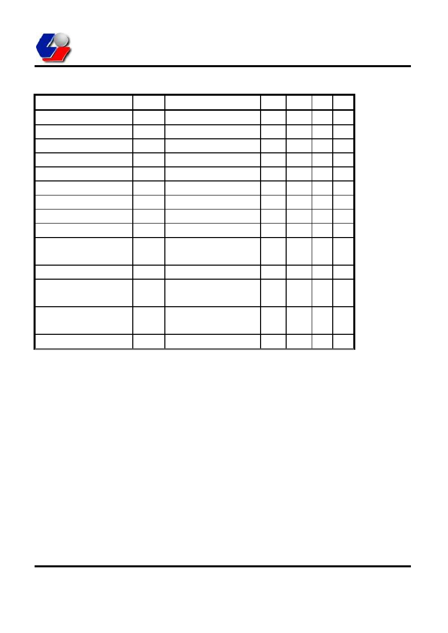
7. ELECTRICAL CHARACTERISTIC :
Parameter
Symbol
Condition
Min Typ. Max Unit
Supply Voltage
Vdd
2.5
3.0
3.5
V
RC oscillation frequency
sys
Vdd=2.7V
400
800
Khz
Operating current
Idd
Vdd=3V,
sys=4Mhz
1.5
mA
Standby current
Istdby Vdd=3V,
sys=4Mhz
1
mA
Sleep mode current
Islp
Vdd=3V
1
�
A
Input high voltage
Vih
Vdd=3.0V
2.0
V
Input low voltage
Vil
Vdd=3.0V
-0.6
0.8
V
Input high leakage current
Iih
Vih=Vdd
1
�
A
Input low leakage current
Iil
Vil=0
-5
�
A
Output high voltage
Voh
Ioh=-2mA
Vdd-
0.4
Vdd
V
Output low voltage
Vol
Iol=4mA
0
0.4
V
Output high voltage
(PWM1, PWM2)
Voh
Vdd=3V, Ioh=-60mA
Vdd-1
Vdd
V
Output low voltage
(PWM1, PWM2)
Vol
Vdd=3V, Iol=75mA
0
1
V
AUD (D/A full scale)
Io
Vdd=3V, Rl=100 OHM
-4.0
mA

Voice Controllerr 19 / 19 Issue Date : 27
March,2000
Syntek Semiconductor Co., Ltd.
STK88C2441
Customer Information Sheet
1. Customer's Name : ____________________
2. Project title : _________________________
3. Syntek part number : ___________________ (will be filled by Syntek)
4. Package --------- ( ) Chip
( ) PDIP
5. Customer code :
Code form ----------
( ) EPROM
( ) file _______________
Checksum ---------- 00000-0FFFF __________H
10000-1FFFF __________H
20000-2FFFF __________H
30000-3FFFF __________H
00000-3FFFF __________H
6. Others :
Customer : __________________ Date : __/__/__
Salesman : __________________ Date : __/__/__